


键盘解码器和I / O扩展 Keypad Decoder and I/O Expansion
Product Details
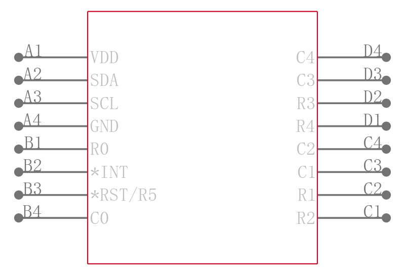
The ADP5585 is a 10I/O port expander with built-in keypad matrix decoder, programmable logic, reset generator, and PWM generator. I/O expander ICs are used in portable devices phones, remote controls, & cameras and non-portable applications healthcare, industrial & instrumentation. I/O expanders can be used to increase the number of I/Os available to a processor or to reduce the number of I/Os required through interface connectors for front panel designs.
The ADP5585 handles all key scanning and decoding and can flag the main processor via an interrupt line that new key events have occurred. GPI changes and logic changes can also be tracked as events via the FIFO, eliminating the need to monitor different registers for event changes. The ADP5585 is equipped with a FIFO to store up to 16 events. Events can be read back by the processor via an I2C compatible interface.
The ADP5585 frees up the main processor from having to monitor the keypad, thereby reducing power consumption and/or increasing processor bandwidth for performing other functions.
The programmable logic functions allow common logic requirements to be integrated as part of the GPIO expander, saving board area and cost.
Applications
- .
- Devices requiring keypad entry and I/O expansion capabilities
### Features and Benefits
- .
- 16 element FIFO for event recording
- .
- 10 configurable I/Os
- .
- Key pad decoding for matrix up to 5x5, with an 11 GPIO 5x6 Option
- .
- Key press/release interrupts
- .
- GPIO functions
- .
- GPI with selectable interrupt level
- .
- 100k/300k pull-up
- .
- 300k pull-down
- .
- GPO with push-pull or open-drain
- .
- Programmable Logic Block
- .
- PWM generator
\- Internal PWM Generation
\- External PWM with internal PWM AND function
- .
- Reset generators
- .
- I2C interface with Fast-mode plus Fm+ support up to 1MHz
- .
- Open drain interrupt output
- .
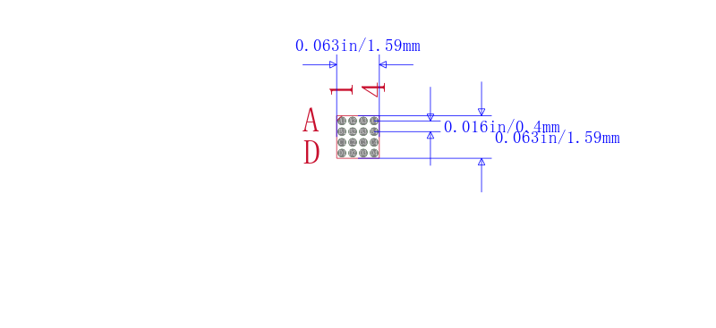
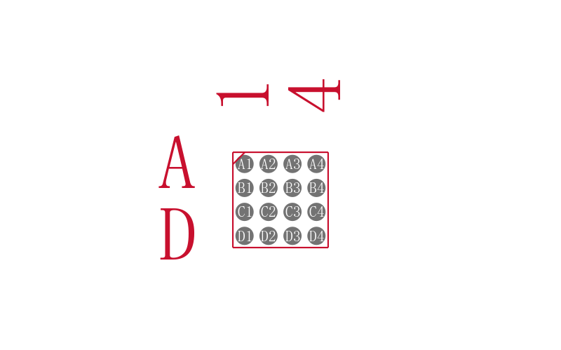
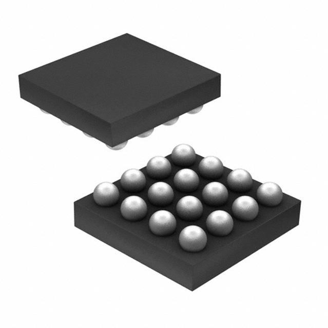
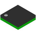
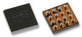
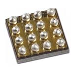
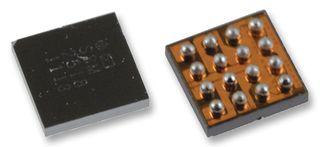
- 16 bump WLCS