跨阻抗放大器 Die Film Frame
Product Details
The ADN3010-11 is a high speed optical receiver featuring a proprietary large area germanium photodiode monolithically integrated with a silicon TIA and LA. The integration of the photodiode eliminates bond wires between the diode and the TIA that provides guaranteed performance and improved manufacturing reliability. The 50 μm diameter photodetector enables an easy optical coupling design when aligned with a single mode fiber SMF. With a 1310 nm optimized ARC, the ADN3010-11 supports 10GBASE-LR and other applications with extended data rates of up to 11.3 Gbps.
Although the ADN3010-11 can operate in the wavelength range from 850 nm to 1565 nm, it has an antireflective coating ARC centered at 1310 nm and is characterized only at original band O band wavelengths 1270 nm, 1290 nm, 1300 nm, 1310 nm, and 1330 nm in this data sheet.
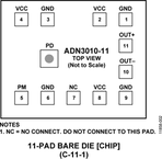
The power monitor pin provides either an output voltage or current that is proportional to the sensed average photocurrent.
Typical power consumption of the ADN3010-11 is 102 mW from a single 3.3 V supply. When the output is saturated, it has a typical differential amplitude of 460 mV p-p at 10.52 Gbps.
The ADN3010-11 is available in die form, and it is operational over the extended industrial temperature range of −40°C to +85°C.
Applications
- .
- Optical module receivers up to 11.3 Gbps
- .
- Short range 10 Gb SONET, FC, Ethernet, CPRI, OBSAI, and LTE optical receivers
- .
- Capable to be in ROSA, BOSA, or MCM packages
### Features and Benefits
- .
- Integrated SiGe PIN photodiode, transimpedance amplifier TIA, and limiting amplifier LA
- .
- Power monitor output: 1.0 A/W at O band wavelengths
- .
- 50 μm diameter germanium photodiode
- .
- Input sensitivity
- .
- POMA = −16.5 dBm
- .
- PAVE = −17.3 dBm ER = 6 dB
- .
- PRBS31 at 10.52 Gbps, BER = 10−12, λ = 1270 nm, 1290 nm, 1300 nm, 1310 nm, and 1330 nm
- .
- Antireflective coating ARC optimized to 1310 nm
- .
- Single 3.3 V supply
- .
- Power dissipation: 102 mW
- .
- Differential output swing: 460 mV p-p
- .
- On-chip power monitor function
- .
- Die size: 0.835 mm × 0.675 mm