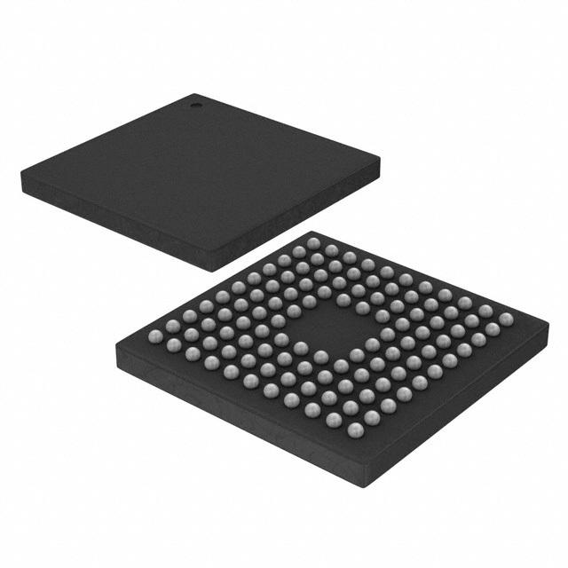
MCU 32Bit ADuCM31x ARM Cortex M3 RISC 256KB Flash 2.5V/3.3V 112Pin CSP-BGA T/R
Product Details
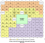
The ADuCM310 is a multidie stack, on-chip system designed for diagnostic control of tunable laser optical module applications. The ADuCM310 features a 16-bit 14-bit accurate multichannel successive approximation register SAR ADC, an ARM Cortex™-M3 processor, eight voltage DACs VDACs, six current output DACs, and Flash/EE memory packaged in a 6 mm × 6 mm, 112-ball CSP_BGA package.
The bottom die in the stack supports the bulk of the low voltage analog circuitry and is the largest of the three die. It contains the ADC, VDACs, main IDAC circuits, as well as other analog support circuits, such as the low drift precision 2.5 V voltage reference source.
The middle die in the stack supports the bulk of the digital circuitry, including the ARM Cortex-M3 processor, the flash and SRAM blocks, and all of the digital communication peripherals. In addition, this die provides the clock sources for the whole chip. A 16 MHz internal oscillator is the source of the internal PLL that outputs an 80 MHz system clock.
The top die, which is the smallest die, was developed on a high voltage process, and this die supports the −5 V and +5 V VDAC outputs. It also implements the SOA IDAC current sink circuit that allows the external SOA diode to pull to a −3.0 V level to implement the fast shutdown of the laser output.
Regarding the individual blocks, the ADC is capable of operating at conversion rates up to 800 kSPS. There are 10 external inputs to the ADC, which can be single ended or differential. Several internal channels are included, such as the supply monitor channels, an on-chip temperature sensor, and internal voltage reference monitors.
The VDACs are 12-bit string DACs with output buffers capable of sourcing between 10 mA and 50 mA, and these DACs are all capable of driving 10 nF capacitive loads.
The low drift current DACs have 14-bit resolution and varied full-scale output ranges from 0 mA to 20 mA to 0 mA to 250 mA on the SOA IDAC IDAC3. The SOA IDAC also comes with a 0 mA to −80 mA current sink capability.
A precision 2.5 V on-chip reference source is available. The internal ADC, IDACs, and VDAC circuits use this on-chip reference source to ensure low drift performance for all of these peripherals.
The ADuCM310 also provides 2× buffered reference outputs capable of sourcing up to 1.2 mA. These outputs can be used externally to the chip.
The ADuCM310 integrates an 80 MHz ARM Cortex-M3 processor. It is a 32-bit reduced instruction set computer RISC machine, offering up to 100 DMIPS peak performance. The ARM Cortex-M3 processor also has a flexible 14-channel direct memory access DMA controller supporting serial peripheral interface SPI, UART, and I2C communication peripherals. The ADuCM310 has 256 kB of nonvolatile Flash/EE memory and 32 kB of SRAM integrated on-chip.
A 16 MHz on-chip oscillator generates the 80 MHz system clock. This clock internally divides to allow the processor to operate at lower frequency, thus saving power. A low power internal 32 kHz oscillator is available and can clock the timers. The ADuCM310 includes three general-purpose timers, a wake-up timer which can be used as a general-purpose timer, and a system watchdog timer.
A range of communication peripherals can be configured as required in a specific application. These peripherals include UART, 2 × I2C, 2 × SPI, GPIO ports, and pulse-width modulation PWM.
On-chip factory firmware supports in-circuit serial download via the UART, while nonintrusive emulation and program download are supported via the serial wire debug port SW-DP interface. These features are supported on the EVAL-ADuCM310QSPZ development system.
The ADuCM310 operates from 2.9 V to 3.6 V and is specified over a temperature range of −40°C to +85°C.
Note that, throughout this data sheet, multifunction pins, such as P1.0/SIN/ECLKIN/PLAI[4], are referred to either by the entire pin name or by a single function of the pin, for example, P1.0, when only that function is relevant.
For additional information on the ADuCM310, see the ADuCM310 reference manual, _How to Set Up and Use the ADuCM310._
### Features and Benefits
- .
- Analog input/output
- .
- 22-channel, 14-bit, 800 kSPS analog-to-digital converter ADC
- .
- 10 external channels
- .
- 1 on-chip die temperature monitor
- .
- 6 current output digital-to-analog converter IDAC monitor channels
- .
- 3 power monitor channels
- .
- 2 buffered reference output channels
- .
- Fully differential and single-ended modes
- .
- 0 V to 2.5 V analog input range
- .
- 6 low noise, 12-/14-bit IDAC outputs
- .
- 1× 250 mA, 1× 200 mA, 2× 100 mA, and 2× 20 mA
- .
- Semiconductor optical amplifier SOA IDAC pull-down to −3.0 V for fast current sink
- .
- Eight 12-bit voltage output DACs VDACs
- .
- Channel 0 and Channel 1: 0 V to 3 V, 75 Ω load
- .
- Channel 2 and Channel 3: −5 V to 0 V, 500 Ω load
- .
- Channel 4 and Channel 5: 0 V to 3 V, 300 Ω load
- .
- Channel 6: 0 V to 5 V, 500 Ω load
- .
- Channel 7: 0 V to 5 V, 100 Ω load
- .
- 2.5 V, on-chip voltage reference
- .
- 2 buffered 2.5 V outputs
- .
- Microcontroller
- .
- ARM Cortex-M3 processor, 32-bit RISC architecture
- .
- Serial wire port supports code download and debugging
- .
- See data sheet for additional features