4/8通道故障保护模拟多路复用器 4/8 Channel Fault-Protected Analog Multiplexers
GENERAL DESCRIPTION
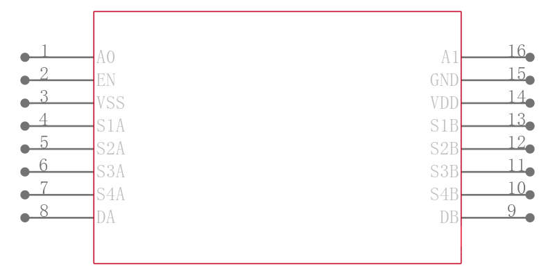
The ADG508F, ADG509F and ADG528F are CMOS analog multiplexers, the ADG508F and ADG528F comprising eight single channels and the ADG509F comprising four differential channels. These multiplexers provide fault protection. Using a series n-channel, p-channel, n-channel MOSFET structure, both device and signal source protection is provided in the event of an overvoltage or power loss. The multiplexer can withstand continuous overvoltage inputs from –40 V to +55 V. During fault conditions, the multiplexer input or output appears as an open circuit and only a few nanoamperes of leakage current will flow. This protects not only the multiplexer and the circuitry driven by the multiplexer, but also protects the sensors or signal sources that drive the multiplexer.
FEATURES
Low On Resistance 300 V typ
Fast Switching Times
tON 250 ns max
tOFF 250 ns max
Low Power Dissipation 3.3 mW max
Fault and Overvoltage Protection –40 V to +55 V
All Switches OFF with Power Supply OFF
Analog Output of ON Channel Clamped Within Power Supplies If an Overvoltage Occurs
Latch-Up Proof Construction
Break Before Make Construction
TTL and CMOS Compatible Inputs
APPLICATIONS
Existing Multiplexer Applications Both Fault-Protected and Nonfault-Protected
New Designs Requiring Multiplexer Functions