Continuous Rate 6.5Mbps to 8.5Gbps Clock and Data Recovery IC with Integrated Limiting Amp/EQ
Product Details
The ADN2913 provides the receiver functions of quantization, signal level detection, and clock and data recovery for continuous data rates from 6.5 Mbps to 8.5 Gbps. The ADN2913 automatically locks to all data rates without the need for an external reference clock or programming. ADN2913 jitter performance exceeds all jitter specifications required by SONET/SDH, including jitter transfer, jitter generation, and jitter tolerance.
The ADN2913 provides manual or automatic slice adjust and manual sample phase adjusts. Additionally, the user can select a limiting amplifier, equalizer, or 0 dB EQ at the input. The equalizer is adaptive or it can be manually set.
The receiver front-end loss of signal LOS detector circuit indicates when the input signal level falls below a user-programmable threshold. The LOS detection circuit has hysteresis to prevent chatter at the LOS output. In addition, the input signal strength can be read through the I2C registers.
The ADN2913 also supports pseudorandom binary sequence PRBS generation, bit error detection, and input data rate readback features.
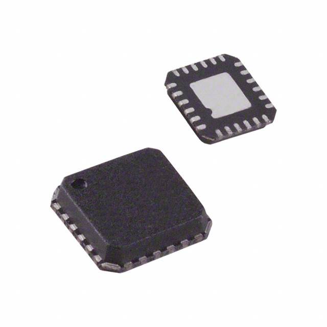
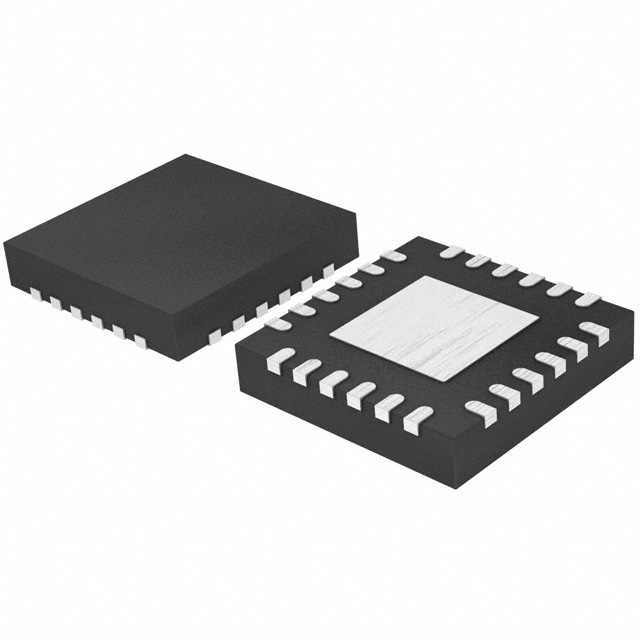
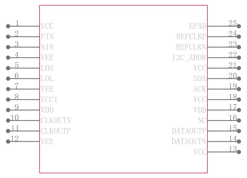
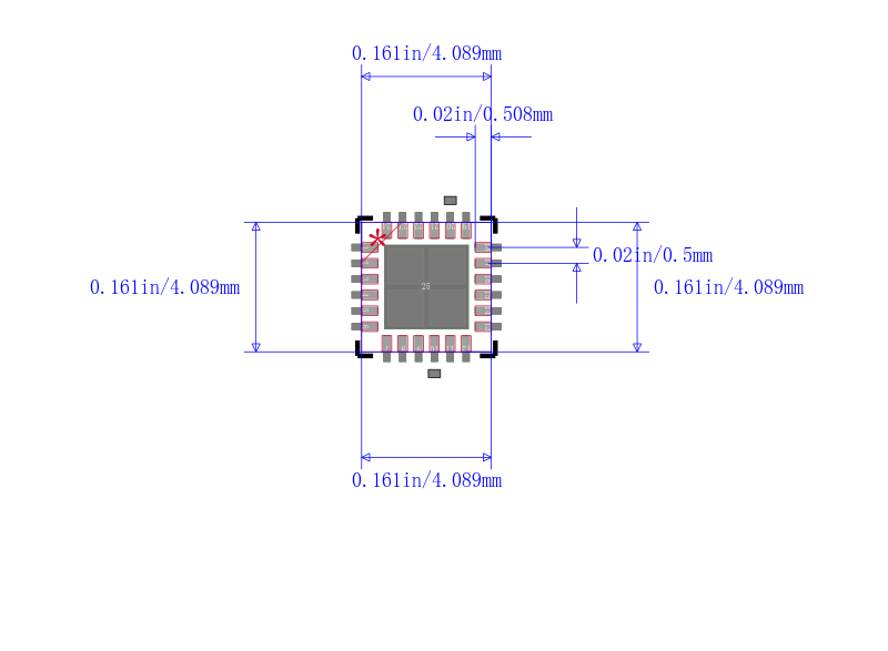
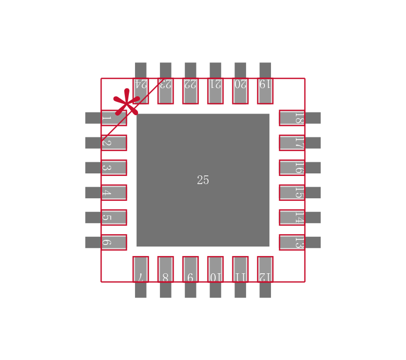
The ADN2913 is available in a compact 4 mm × 4 mm, 24-lead lead frame chip scale package LFCSP. All ADN2913 specifications are defined over the ambient temperature range of −40°C to +85°C, unless otherwise noted.
**Applications**
- .
- SONET/SDH OC-1/OC-3/OC-12/OC-48 and all associated FEC rates
- .
- 1GE, 1GFC, 2GFC, 4GFC, 8GFC, CPRI OS/L.6 up to OS/L.60
- .
- Any rate regenerators/repeaters
### Features and Benefits
- .
- Serial data input: 6.5 Mbps to 8.5 Gbps
- .
- No reference clock required
- .
- Exceeds SONET/SDH requirements for jitter transfer/ generation/tolerance
- .
- Quantizer sensitivity: 6.3 mV typical limiting amplifier mode
- .
- Optional limiting amplifier, equalizer EQ, and 0 dB EQ inputs
- .
- Programmable jitter transfer bandwidth to support G.8251 OTN
- .
- Programmable slice level
- .
- Sample phase adjust 5.65 Gbps or greater
- .
- Output polarity invert
- .
- Programmable LOS threshold via I2C
- .
- I2C interface to access optional features
- .
- Loss of signal LOS alarm limiting amplifier mode only
- .
- Loss of lock LOL indicator
- .
- PRBS generator/detector
- .
- Application aware power
- .
- 352 mW at 8.5 Gbps, equalizer mode, no clock output
- .
- 380 mW at 6.144 Gbps, limiting amplifier mode, no clock output
- .
- 340 mW at 622 Mbps, 0 dB EQ mode, no clock output
- .
- Power supplies: 1.2 V, flexible 1.8 V to 3.3 V, and 3.3 V
- .
- 4 mm × 4 mm, 24-lead LFCSP

| 型号/品牌 | 代替类型 | 替代型号对比 |
|---|---|---|
ADN2913ACPZ-RL7 ADI 亚德诺 | 当前型号 | 当前型号 |
ADN2913ACPZ 亚德诺 | 完全替代 | ADN2913ACPZ-RL7和ADN2913ACPZ的区别 |