
CMOS 300 MHz的完整DDS CMOS 300 MHz Complete-DDS
GENERAL DESCRIPTION
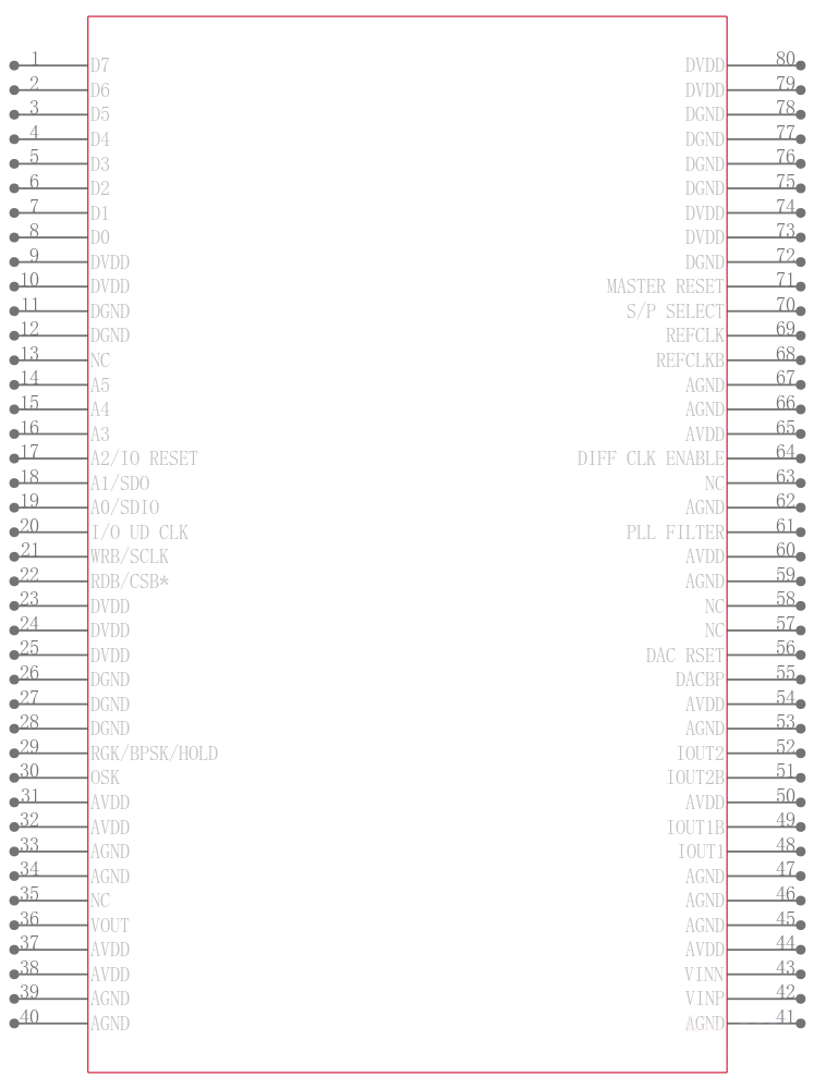
The AD9852 digital synthesizer is a highly integrated device that uses advanced DDS technology, coupled with an internal high speed, high performance D/A converter to form a digitally programmable, agile synthesizer function. When referenced to an accurate clock source, the AD9852 generates a highly stable frequency-, phase-, and amplitude-programmable cosine output that can be used as an agile LO in communications, radar, and many other applications. The innovative high speed DDS core of the AD9852 provides 48-bit frequency resolution 1 μHz tuning resolution with 300 MHz SYSCLK. Maintaining 17 bits ensures excellent SFDR.
FEATURES
300 MHz internal clock rate
FSK, BPSK, PSK, chirp, AM operation
Dual integrated 12-bit D/A converters
Ultrahigh speed comparator, 3 ps rms jitter
Excellent dynamic performance 80 dB SFDR at 100 MHz ±1 MHz AOUT
4× to 20× programmable reference clock multiplier
Dual 48-bit programmable frequency registers
Dual 14-bit programmable phase offset registers
12-bit programmable amplitude modulation and on/off output shaped keying function
Single-pin FSK and BPSK data interfaces
PSK capability via I/O interface
Linear or nonlinear FM chirp functions with single pin frequency hold function
Frequency ramped FSK
<25 ps rms total jitter in clock generator mode
Automatic bidirectional frequency sweeping
Sinx/x correction
Simplified control interface
10 MHz serial 2-wire or 3-wire SPI-compatible
100 MHz parallel 8-bit programming
3.3 V single supply
Multiple power-down functions
Single-ended or differential input reference clock
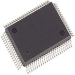
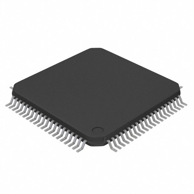
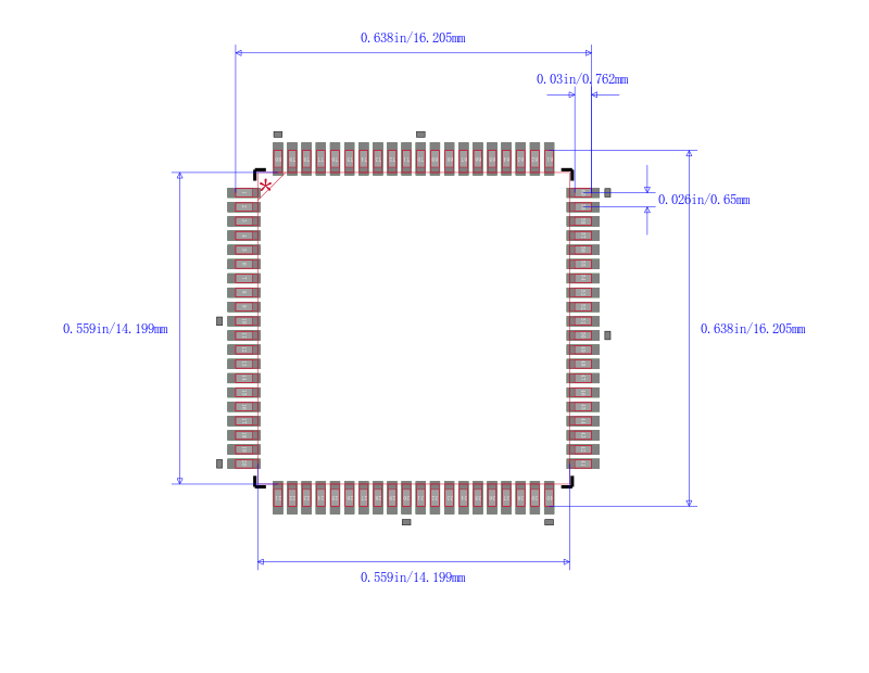
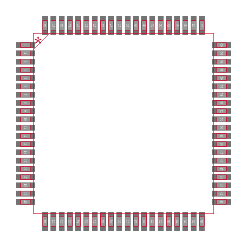
Small, 80-lead LQFP or TQFP with exposed pad
APPLICATIONS
Agile LO frequency synthesis
Programmable clock generator
FM chirp source for radar and scanning systems
Test and measurement equipment
Commercial and amateur RF exciter
| 型号/品牌 | 代替类型 | 替代型号对比 |
|---|---|---|
AD9852AST ADI 亚德诺 | 当前型号 | 当前型号 |
ADF4210BRU 亚德诺 | 类似代替 | AD9852AST和ADF4210BRU的区别 |
AD9852ASTZ 亚德诺 | 功能相似 | AD9852AST和AD9852ASTZ的区别 |
AD800-52BRZRL 亚德诺 | 功能相似 | AD9852AST和AD800-52BRZRL的区别 |