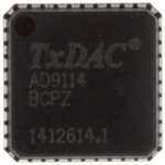

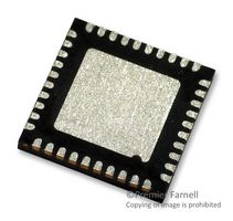
ANALOG DEVICES AD9114BCPZ 数模转换器, 双路, 8 bit, 125 MSPS, 串行, 1.7V 至 3.5V, LFCSP, 40 引脚
Product Details
The AD9114/AD9115/AD9116/AD9117 are pin-compatible dual, 8-/10-/12-/14-bit, low power digital-to-analog converters DACs that provide a sample rate of 125 MSPS. These TxDAC® converters are optimized for the transmit signal path of commu-nication systems. All the devices share the same interface, package, and pinout, providing an upward or downward component selection path based on performance, resolution, and cost.
The AD9114/AD9115/AD9116/AD9117 offer exceptional ac and dc performance and support update rates up to 125 MSPS.
The flexible power supply operating range of 1.8 V to 3.3 V and low power dissipation of the AD9114/AD9115/AD9116/AD9117 make them well suited for portable and low power applications.
**Product Highlights**
1. Low Power. DACs operate on a single 1.8 V to 3.3 V supply; total power consumption reduces to 225 mW at 100 MSPS. Sleep and power-down modes are provided for low power idle periods.
2. CMOS Clock Input. High speed, single-ended CMOS clock input supports a 125 MSPS conversion rate.
3. Easy Interfacing to Other Components. Adjustable output common mode from 0 V to 1.2 V allows for easy interfacing to other components that accept common-mode levels greater than 0 V.
**Applications**
- .
- Wireless infrastructures
Picocell, femtocell base stations
- .
- Medical instrumentation
Ultrasound transducer excitation
- .
- Portable instrumentation
Signal generators, arbitrary waveform generators
### Features and Benefits
- .
- Power dissipation @ 3.3 V, 20 mA output
191 mW @ 10 MSPS
232 mW @ 125 MSPS
- .
- Sleep mode: <3 mW @ 3.3 V
- .
- Supply voltage: 1.8 V to 3.3 V
- .
- SFDR to Nyquist
86 dBc @ 1 MHz output
85 dBc @ 10 MHz output
- .
- NSD @ 10 MHz output, 125 MSPS, 20 mA: −132 dBc/Hz
|
- .
- Differential current outputs: 4 mA to 20 mA
- .
- 2 on-chip auxiliary DACs
- .
- CMOS inputs with single-port operation
- .
- Output common mode: adjustable 0 V to 1.2 V
- .
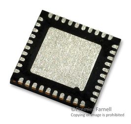
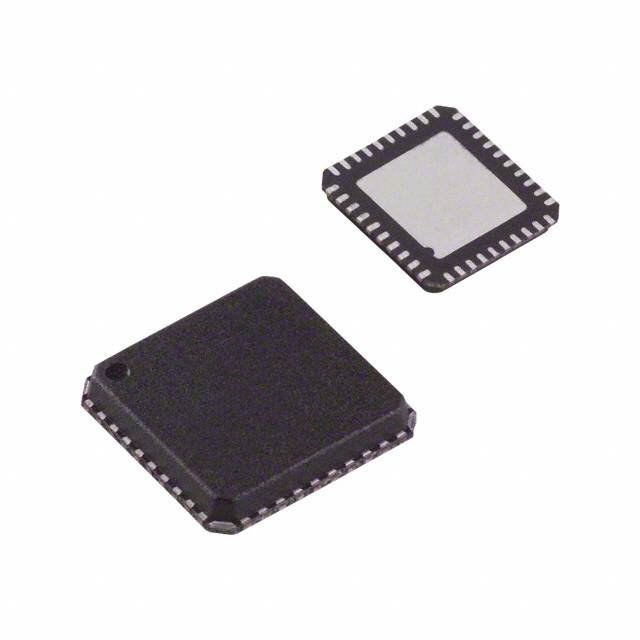
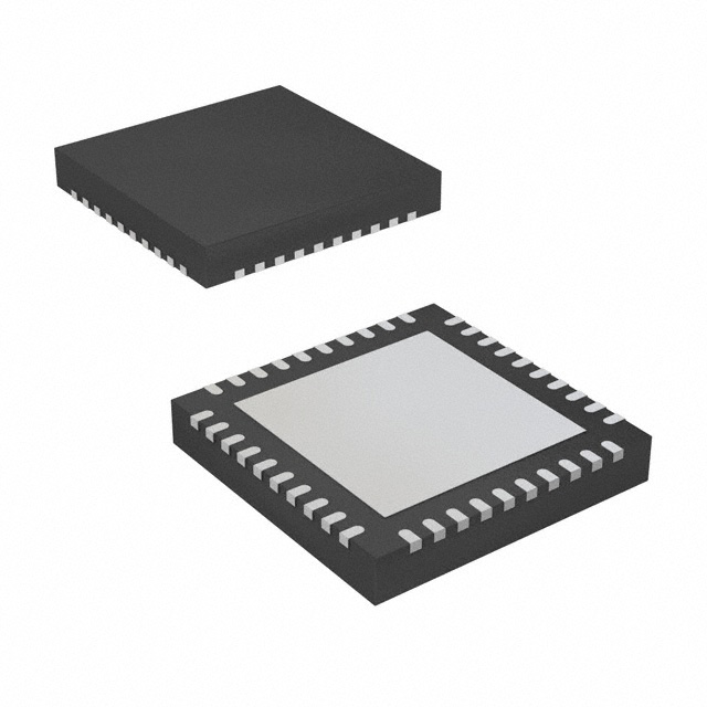
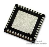
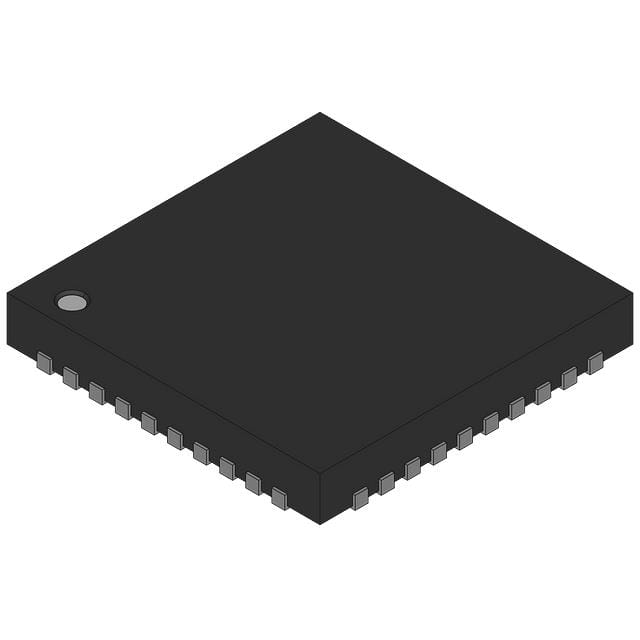
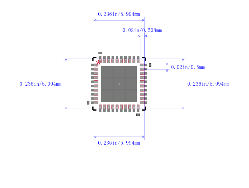
- Small footprint 40-lead LFCSP RoHS-compliant package
---|---
输出接口数 2
供电电流 55.0 mA
通道数 2
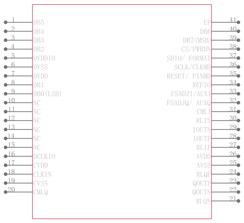
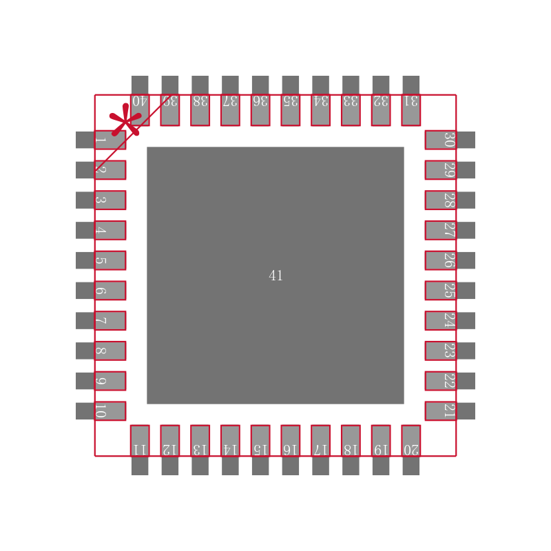
针脚数 40
位数 8
耗散功率 232 mW
采样率 125 Msps
分辨率Bits 8.0
工作温度Max 85 ℃
工作温度Min -40 ℃
耗散功率Max 232 mW
数模转换数DAC 2
电源电压 1.7V ~ 3.5V
安装方式 Surface Mount
引脚数 40
封装 LFCSP-40
高度 0.83 mm
封装 LFCSP-40
工作温度 -40℃ ~ 85℃
产品生命周期 Active
包装方式 Tray
RoHS标准 RoHS Compliant
含铅标准 Lead Free
REACH SVHC标准 No SVHC
军工级 No
REACH SVHC版本 2015/12/17
ECCN代码 EAR99

| 型号/品牌 | 代替类型 | 替代型号对比 |
|---|---|---|
AD9114BCPZ ADI 亚德诺 | 当前型号 | 当前型号 |
AD9114BCPZRL7 亚德诺 | 功能相似 | AD9114BCPZ和AD9114BCPZRL7的区别 |