
ANALOG DEVICES AD9121BCPZ 数模转换器, 14 bit, 1.23 GSPS, 串行, 3.13V 至 3.47V, LFCSP, 72 引脚
Product Details
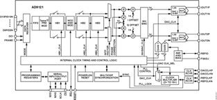
The AD9121 is a dual, 14-bit, high dynamic range digital-to-analog converter DAC that provides a sample rate of 1230 MSPS, permitting multicarrier generation up to the Nyquist frequency.
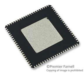
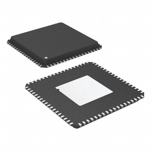
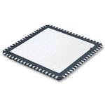
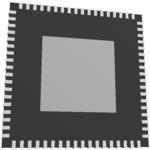
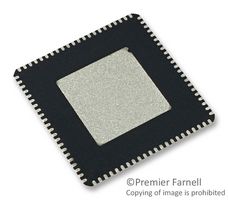
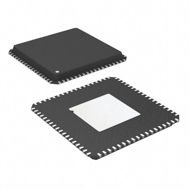
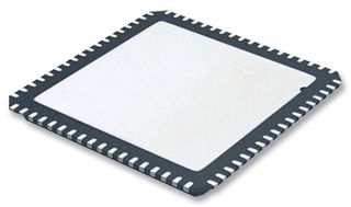
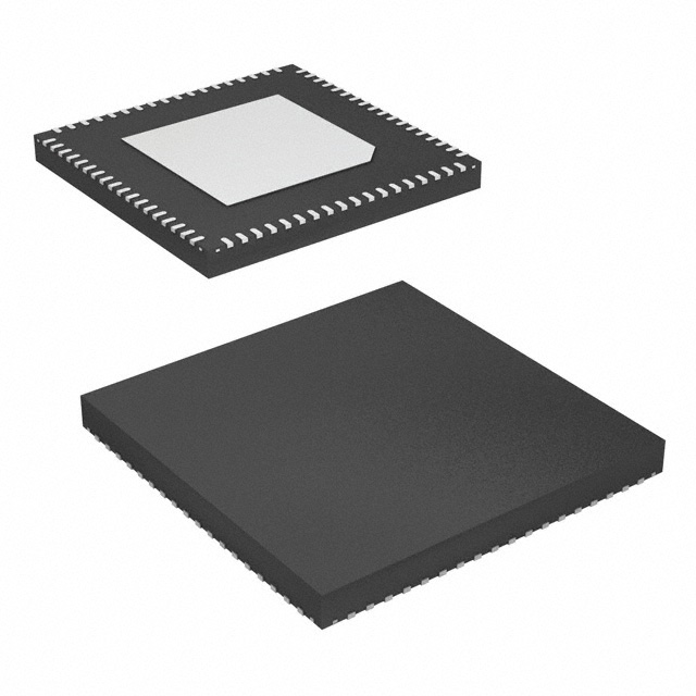
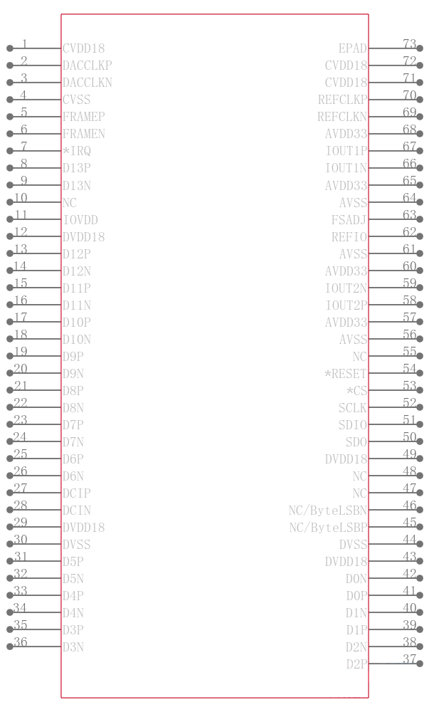
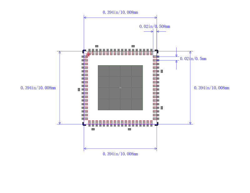
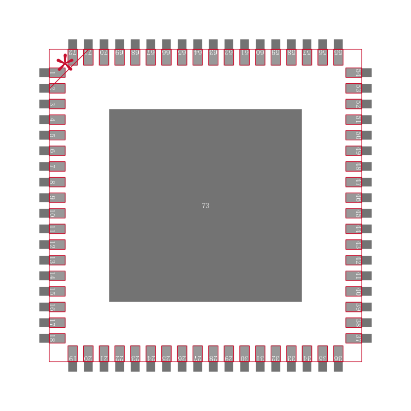
The AD9121 TxDAC+® includes features optimized for direct conversion transmit applications, including complex digital modulation, and gain and offset compensation. The DAC outputs are optimized to interface seamlessly with analog quadrature modulators, such as the ADL537x F-MOD series from Analog Devices, Inc. A 4-wire serial port interface provides for programming/readback of many internal parameters. Full-scale output current can be programmed over a range of 8.7 mA to 31.7 mA. The AD9121 comes in a 72-lead LFCSP.
**Product Highlights**
1. Ultralow noise and intermodulation distortion IMD enable high quality synthesis of wideband signals from baseband to high intermediate frequencies IF.
2. Proprietary DAC output switching technique enhances dynamic performance.
3. Current outputs are easily configured for various single-ended or differential circuit topologies.
4. Flexible LVDS digital interface allows the standard 28-wire bus to be reduced to one-half of the width.
**
**
Applications- .
- *
**
- .
- Wireless infrastructure
- .
- W-CDMA, CDMA2000, TD-SCDMA, WiMAX, GSM, LTE
- .
- Digital high or low IF synthesis
- .
- Transmit diversity
- .
- Wideband communications: LMDS/MMDS, point-to-point
### Features and Benefits
- .
- Flexible LVDS interface allows word or byte load
- .
- Single-carrier W-CDMA ACLR = 82 dBc at 122.88 MHz IF
- .
- Analog output: adjustable 8.7 mA to 31.7 mA, RL = 25 Ω to 50 Ω
- .
- Integrated 2×/4×/8× interpolator/complex modulator allows carrier placement anywhere in the DAC bandwidth
- .
- Gain, dc offset, and phase adjustment for sideband suppression
- .
- Multiple chip synchronization interfaces
- .
- High performance, low noise PLL clock multiplier
- .
- Digital inverse sinc filter
- .
- Low power: 1.5 W at 1.2 GSPS, 800 mW at 500 MSPS, full operating conditions
- .
- 72-lead, exposed paddle LFCSP
输出接口数 2
通道数 2
针脚数 72
位数 14
采样率 1.23 GHz
工作温度Max 85 ℃
工作温度Min -40 ℃
数模转换数DAC 2
电源电压 3.13V ~ 3.47V
安装方式 Surface Mount
引脚数 72
封装 LFCSP-72
高度 0.83 mm
封装 LFCSP-72
工作温度 -40℃ ~ 85℃
产品生命周期 Active
包装方式 Cut Tape CT
制造应用 Aerospace and Defense, Radar
RoHS标准 RoHS Compliant
含铅标准 Contains Lead
REACH SVHC标准 No SVHC
REACH SVHC版本 2015/12/17
| 型号/品牌 | 代替类型 | 替代型号对比 |
|---|---|---|
AD9121BCPZ ADI 亚德诺 | 当前型号 | 当前型号 |
AD9121BCPZRL 亚德诺 | 完全替代 | AD9121BCPZ和AD9121BCPZRL的区别 |