


ANALOG DEVICES AD5694RBCPZ-RL7 数模转换器, 四路, 12 bit, 串行, 2.7V 至 5.5V, LFCSP, 16 引脚
Product Details
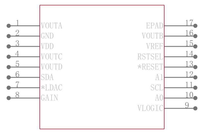
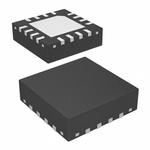
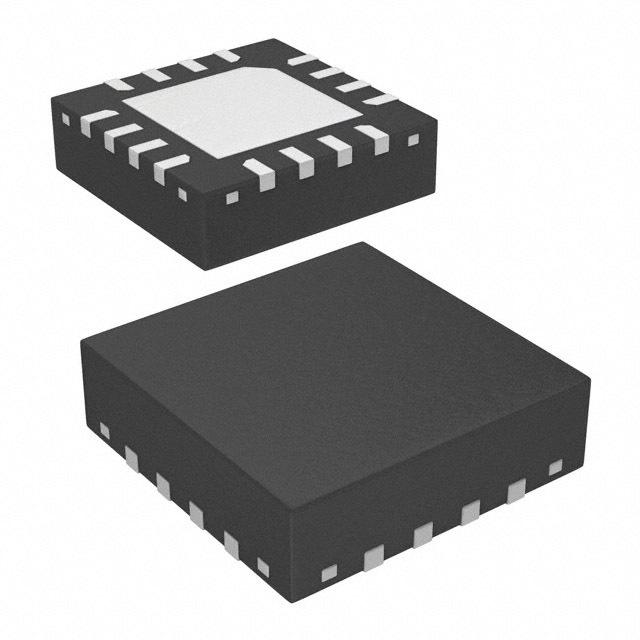
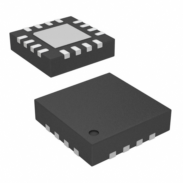
The AD5694R is a low power, quad, 16-bit buffered voltage output DAC. The device includes a 2.5 V, 2 ppm/°C internal reference enabled by default and a gain select pin giving a full-scale output of 2.5 V gain = 1 or 5 V gain = 2. The device operates from a single 2.7 V to 5.5 V supply, is guaranteed monotonic by design, and exhibits less than 0.1% FSR gain error and 1.5 mV offset error performance. The device is available in a 3 mm × 3 mm LFCSP and a TSSOP package.
The AD5694R also incorporates a power-on reset circuit and a RSTSEL pin that ensures that the DAC outputs power up to zero scale or midscale and remain there until a valid write takes place. Each part contains a per-channel power-down feature that reduces the current consumption of the device to 4 μA at 3 V while in power-down mode.
The AD5694R uses a versatile 2-wire serial interface that operates at clock rates up to 400 kHz, and includes a VLOGIC pin intended for 1.8 V/3 V/5 V logic.
**Product Highlights**
1. High Relative Accuracy INL.
AD5694R 12-bit: ±1 LSB maximum.
2. Low Drift 2.5 V On-Chip Reference.
2 ppm/°C typical temperature coefficient.
5 ppm/°C maximum temperature coefficient.
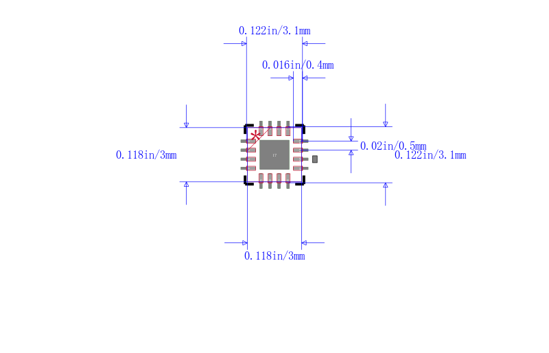
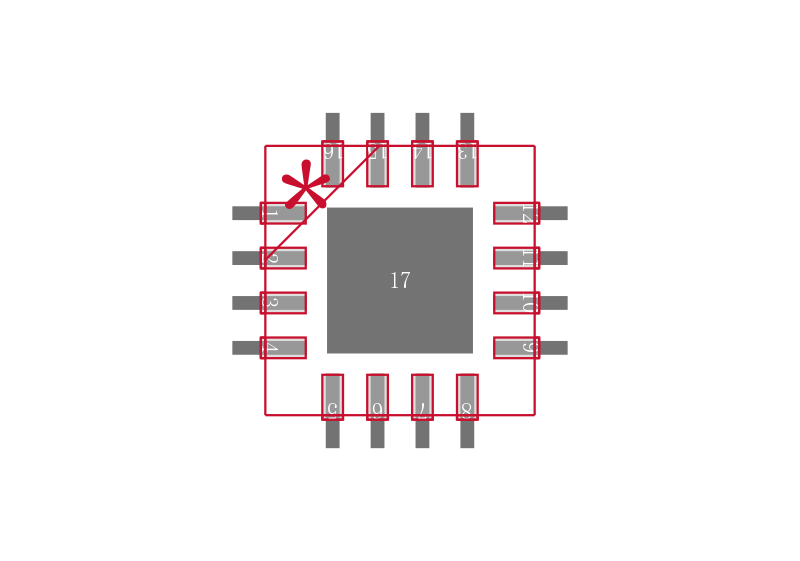
3. Two Package Options.
3 mm × 3 mm, 16-lead LFCSP.
16-lead TSSOP.
**Applications**
- .
- Optical transceivers
- .
- Base-station power amplifiers
- .
- Process control PLC I/O cards
- .
- Industrial automation
- .
- Data acquisition systems
### Features and Benefits
- .
- High relative accuracy INL: ±2 LSB maximum at 16 bits
- .
- Low drift 2.5 V reference: 2 ppm/°C typical
- .
- Tiny package: 3 mm × 3 mm, 16-lead LFCSP
- .
- Total unadjusted error TUE: ±0.1% of FSR maximum
- .
- Offset error: ±1.5 mV maximum
- .
- Gain error: ±0.1% of FSR maximum
- .
- High drive capability: 20 mA, 0.5 V from supply rails
- .
- User selectable gain of 1 or 2 GAIN pin
- .
- Reset to zero scale or midscale RSTSEL pin
- .
- 1.8 V logic compatibility
- .
- Low glitch: 0.5 nV-sec
- .
- 400 kHz I2C-compatible serial interface
- .
- Low power: 3.3 mW at 3 V
- .
- 2.7 V to 5.5 V power supply
- .
- −40°C to +105°C temperature range
输出接口数 4
通道数 4
针脚数 16
位数 12
耗散功率 7.20 mW
分辨率Bits 12.0
工作温度Max 105 ℃
工作温度Min -40 ℃
数模转换数DAC 4
电源电压 2.7V ~ 5.5V
电源电压Max 5.5 V
电源电压Min 2.7 V
安装方式 Surface Mount
引脚数 16
封装 LFCSP-16
高度 0.73 mm
封装 LFCSP-16
工作温度 -40℃ ~ 105℃
产品生命周期 Active
包装方式 Tape & Reel TR
RoHS标准 RoHS Compliant
含铅标准 Contains Lead
REACH SVHC标准 No SVHC
军工级 No
ECCN代码 EAR99