


ANALOG DEVICES ADP8866ACPZ-R7. 芯片, 发光二极管驱动器, LFCSP-20
Product Details
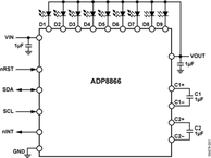
The ADP8866 combines a programmable backlight LED charge pump driver with automatic blinking functions. Nine LED drivers can be independently programmed at currents up to 25 mA. The current level, fade time, and blinking rate can be programmed once and executed autonomously on a loop. Separate fade in and out times can be set for the backlight LEDs.
Driving all of this is a two capacitor charge pump with gains of 1×, 1.5×, and 2×. This setup is capable of driving a maximum IOUT of 240 mA from a supply of 2.5 V to 5.5 V. A full suite of safety features including short-circuit, overvoltage, and over-temperature protection allow easy implementation of a safe and robust design. Additionally, input inrush currents are limited via an integrated soft start combined with controlled input to output isolation.
### Features and Benefits
- .
- Charge pump with automatic gain selection of 1x, 1.5x, and 2x for maximum efficiency.
- .
- 92% peak efficiency
- .
- 9 independent and programmable LED drivers
- .
- Each driver capable of 25 mA full scale
- .
- Each driver has 7 bits 128 levels of non-linear current settings
- .
- Standby mode for <1 μA current consumption
- .
- 16 programmable fade in and fade out times 0.0 sec to 1.75 sec with choice of square or cubic rates
- .
- Automated and customizable LED blinking for all 9 channels.
- .
- Unique heartbeat mode for customizable double pulse lighting effects
- .
- PWM input for implementing content adjustable brightness control CABC
- .
- I2C compatible interface for all programming
- .
- Dedicated reset pin and built-in power on reset POR
- .
- Short circuit, overvoltage, and overtemperature protection
- .
- Internal soft start to limit inrush currents
- .
- Input to output isolation during faults or shutdown
- .
- Operates down to VIN = 2.5 V, with undervoltage lockout UVLO at 2.0 V
- .
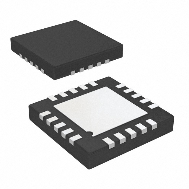
- Small lead frame chip scale package LFCSP
频率 1 MHz
输出接口数 1
输入电压DC 2.50V ~ 5.50V
输出电压 4.9 V
输出电流 25 mA
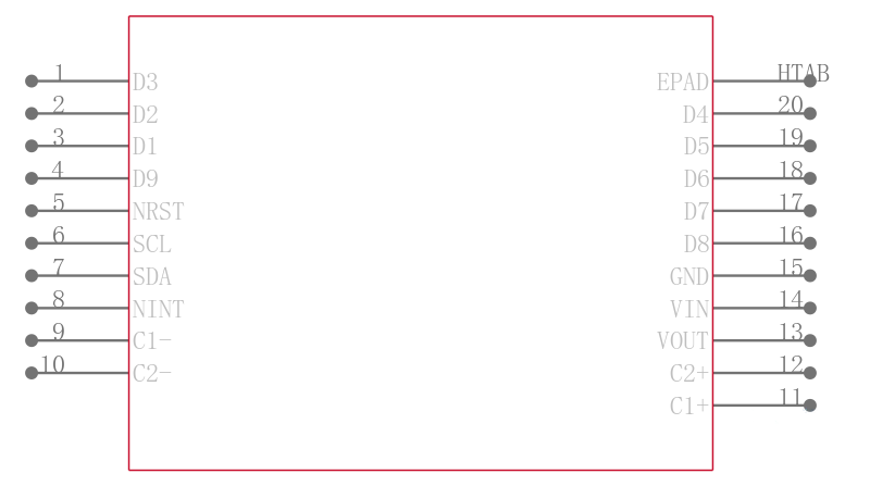
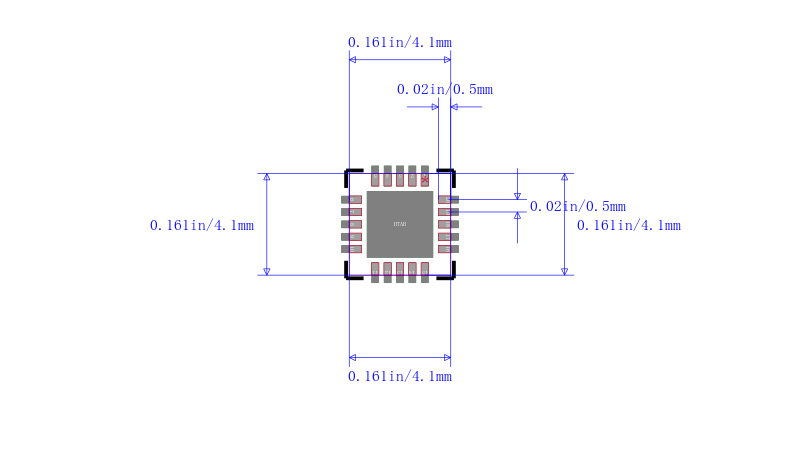
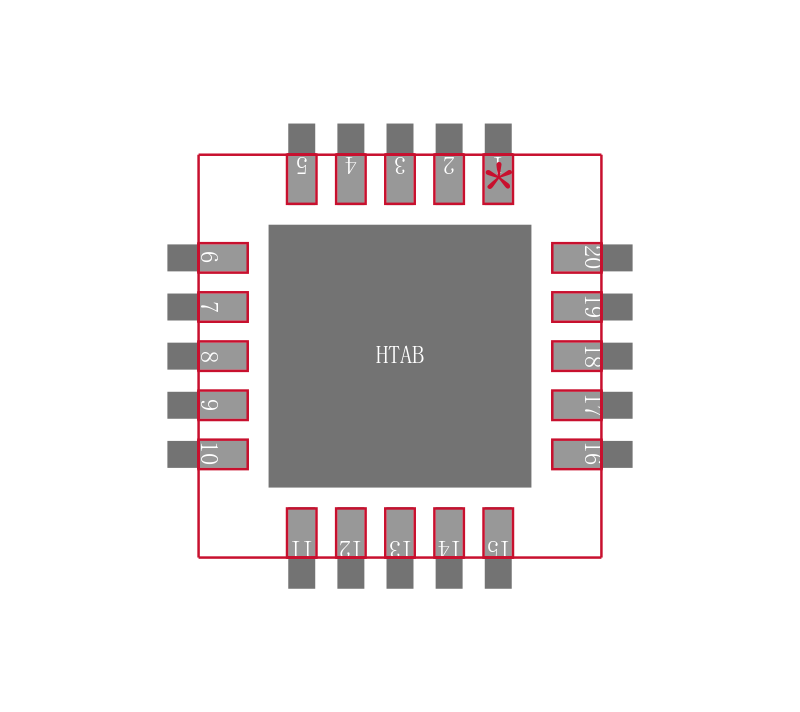
针脚数 20
开关频率 1 MHz
输入电压Max 5.5 V
输入电压Min 2.5 V
工作温度Max 105 ℃
工作温度Min -40 ℃
电源电压 2.5V ~ 5.5V
电源电压Max 5.5 V
电源电压Min 2.5 V
输入电压 2.5V ~ 5.5V
安装方式 Surface Mount
引脚数 20
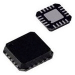
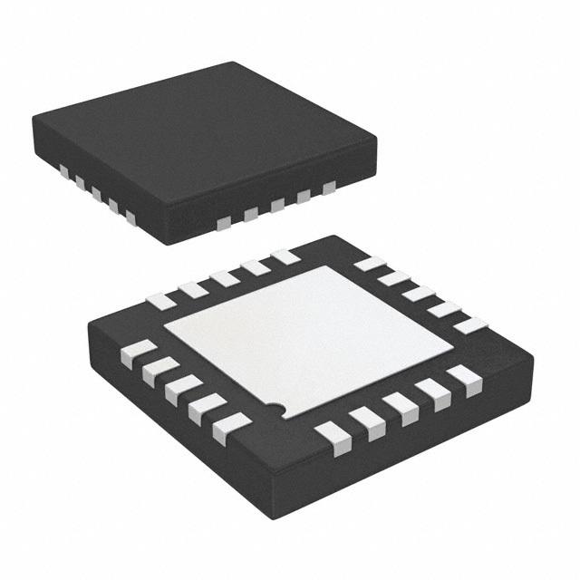
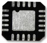
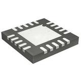
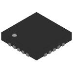
封装 LFCSP-20
长度 4 mm
宽度 4 mm
封装 LFCSP-20
工作温度 -40℃ ~ 85℃ TA
产品生命周期 Active
包装方式 Tape & Reel TR
制造应用 背光
RoHS标准 RoHS Compliant
含铅标准 Lead Free
REACH SVHC标准 No SVHC
REACH SVHC版本 2015/12/17
ECCN代码 EAR99