

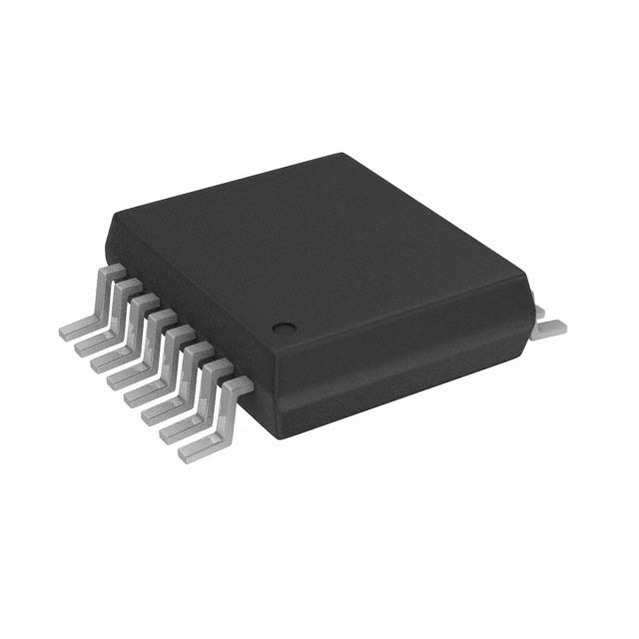
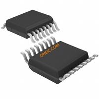

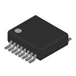
IC,D/A CONVERTER,SINGLE,16Bit,SSOP,16Pin
Product Details
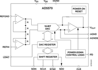
The AD5570 is a single 16-bit serial input, voltage output DAC that operates from supply voltages of ±11.4 V up to ±16.5 V. Integral linearity INL and differential nonlinearity DNL are accurate to 1 LSB. During power-up, when the supply voltages are changing, VOUT is clamped to 0 V via a low impedance path.
The AD5570 DAC comes complete with a set of reference buffers. The reference buffers allow a single, positive reference to be used. The voltage on REFIN is gained up and inverted internally to give the positive and negative reference for the DAC core. Having the reference buffers on-chip eliminates the need for external components such as inverters, precision amplifiers, and resistors, thereby reducing the overall solution size and cost.
The AD5570 uses a versatile 3-wire interface that is compatible with SPI®, QSPI™, MICROWIRE™, and DSP® interface standards. Data is presented to the part as a 16-bit serial word. Serial data is available on the SDO pin for daisy-chaining purposes. Data readback allows the user to read the contents of the DAC register via the SDO pin.
Features on the AD5570 include LDAC which is used to update the output of the DAC. The device also has a power-down pin PD, allowing the DAC to be put into a low power state, and a CLR pin that allows the output to be cleared to 0 V.
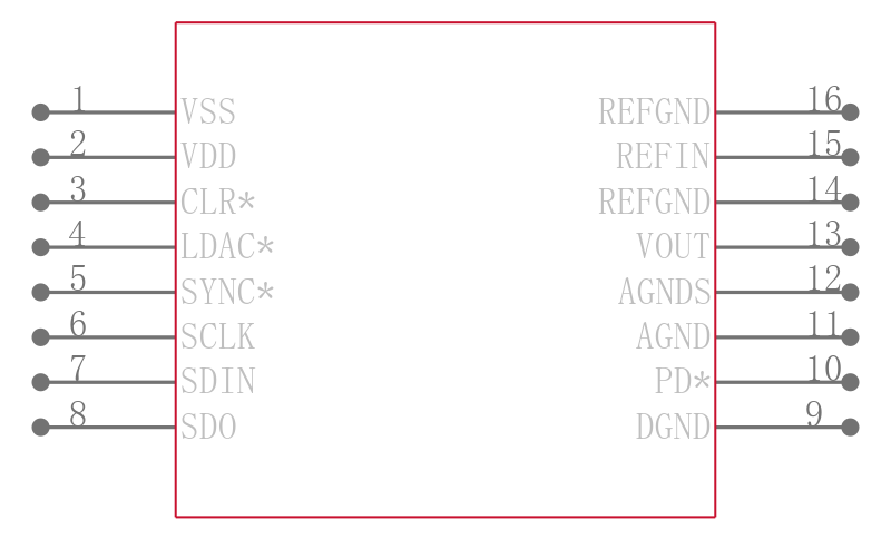
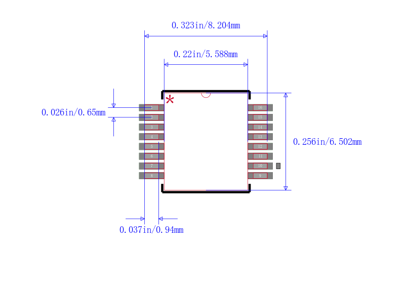
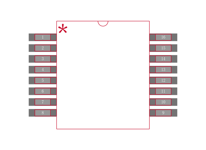
The AD5570 is available in a 16-lead SSOP.
**Product Highlights**
1. 1 LSB maximum INL and DNL.
2. Buffered voltage output up to ±14 V.
3. Output controlled during power-up.
4. On-board reference buffers.
5. Wide temperature range of −40°C to +125°C.
**Applications**
* Industrial automation
* Automatic test equipment
* Process control
* Data acquisition systems
* General-purpose instrumentation
### Features and Benefits
- .
- Full 16-bit performance
- .
- 1 LSB max INL and DNL
- .
- Output voltage range up to ±14 V
- .
- On-board reference buffers, eliminating the need for a negative reference
- .
- Temperature ranges of −40°C to +85°C for A/B version/−40°C to +125°C for W/Y version
- .
- Controlled output during power-on
- .
- Settling time of 10 µs to 0.003%
- .
- Clear function to 0 V
- .
- Asynchronous update of outputs LDAC pin
- .
- Power-on reset
- .
- Serial data output for daisy chaining
- .
- Data readback facility
| 型号/品牌 | 代替类型 | 替代型号对比 |
|---|---|---|
AD5570WRSZ-REEL7 ADI 亚德诺 | 当前型号 | 当前型号 |
AD5570WRS-REEL7 亚德诺 | 完全替代 | AD5570WRSZ-REEL7和AD5570WRS-REEL7的区别 |
AD5570WRSZ 亚德诺 | 类似代替 | AD5570WRSZ-REEL7和AD5570WRSZ的区别 |
AD5570WRS 亚德诺 | 类似代替 | AD5570WRSZ-REEL7和AD5570WRS的区别 |