
数模转换器- DAC 16-bit 2.0Gsps Quad DAC with JESD204B
Product Details
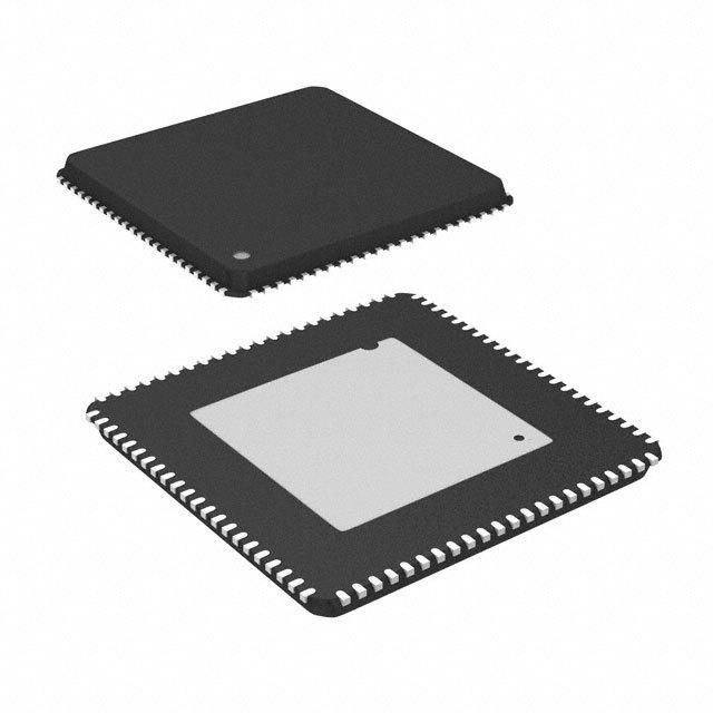
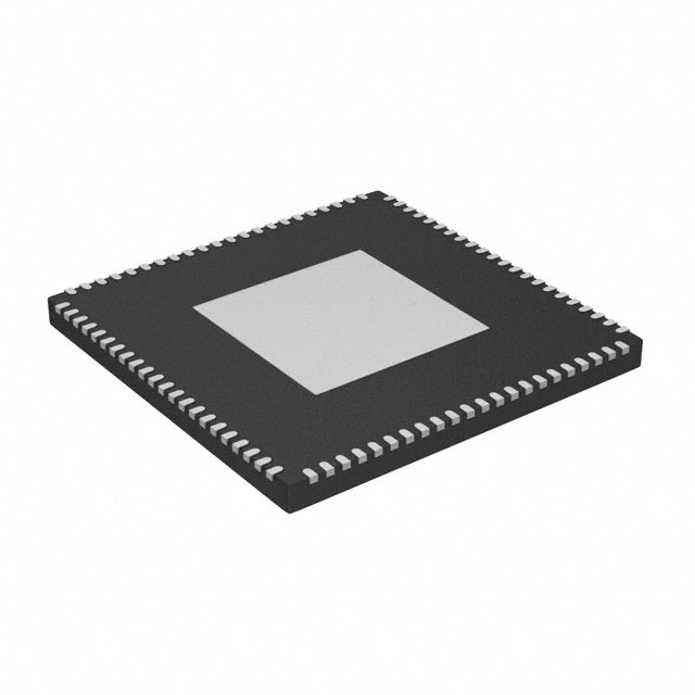
The AD9154 is a quad, 16-bit, high dynamic range digital-to-analog converter DAC that provides a maximum sample rate of 2.4 GSPS, permitting multicarrier generation up to the Nyquist frequency in baseband mode. The AD9154 includes features optimized for direct conversion transmit applications including complex digital modulation, input signal power detection, and gain, phase, and offset compensation. The DAC outputs are optimized to interface seamlessly with the ADRF6720-27 radio frequency quadrature modulator AQM from Analog Devices, Inc. In mix mode, the AD9154 DAC can reconstruct carriers in the second and third Nyquist Zones. A serial port interface SPI provides the programming/readback of internal parameters. The full-scale output current can be programmed over a range of 4 mA to 20 mA. The AD9154 is available in two different 88-lead LFCSP packages
** Product Highlights
**
1. Ultrawide signal bandwidth enables emerging wideband and multiband wireless applications.
2. Advanced low spurious and distortion design techniques provide high quality synthesis of wideband signals from baseband to high intermediate frequencies.
3. JESD204B Subclass 1 support simplifies multichip synchronization.
4. Small package size with a 12 mm × 12 mm footprint.
** Applications
**
- .
- Wireless communications
Multicarrier LTE and GSM base stations
Wideband repeaters
Software defined radios
- .
- Wideband communications
Point to point microwave radio
- .
- Transmit diversity, multiple input/multiple output MIMO
- .
- Instrumentation
- .
- Automated test equipment
### Features and Benefits
- .
- Supports input data rates up to 1 GSPS
- .
- Proprietary, low spurious and distortion design
- .
- Single carrier LTE 20 MHz bandwidth BW, ACLR = 77 dBc at 180 MHz IF
- .
- Six carrier GSM IMD = 78 dBc, 600 kHz carrier spacing at 180 MHz IF
- .
- SFDR = 72 dBc at 180 MHz IF, −6 dBFS single tone
- .
- Flexible 8-lane JESD204B interface
- .
- Multiple chip synchronization
- .
- Fixed latency
- .
- Data generator latency compensation
- .
- Input signal power detection
- .
- High performance, low noise phase-locked loop PLL clock multiplier
- .
- Digital inverse sinc filter
- .
- Digital quadrature modulation using a numerically controlled oscillator NCO
- .
- Nyquist band selection—mix mode
- .
- Selectable 1×, 2×, 4×, and 8× interpolation filters
- .
- Low power: 2.11 W at 1.6 GSPS, full operating conditions
- .
- 88-lead, exposed pad LFCSP

| 型号/品牌 | 代替类型 | 替代型号对比 |
|---|---|---|
AD9154BCPZRL ADI 亚德诺 | 当前型号 | 当前型号 |