
ANALOG DEVICES ADP5071ACPZ 芯片, 直流/直流转换器, 升压/反相, LFCSP-20
Product Details
The ADP5071 is a dual high performance dc-to-dc regulator that generates independently regulated positive and negative rails.
The input voltage range of 2.85 V to 15 V supports a wide variety of applications. The integrated main switch in both regulators enables generation of an adjustable positive output voltage up to +39 V and a negative output voltage down to −39 V below input voltage.
The ADP5071 operates at a pin selected 1.2 MHz/2.4 MHz switching frequency. The ADP5071 can synchronize with an external oscillator from 1.0 MHz to 2.6 MHz to ease noise filtering in sensitive applications. Both regulators implement programmable slew rate control circuitry for the MOSFET driver stage to reduce electromagnetic interference EMI.
Flexible start-up sequencing is provided with the options of manual enable, simultaneous mode, positive supply first, and negative supply first.
The ADP5071 includes a fixed internal or resistor programmable soft start timer to prevent inrush current at power-up. During shutdown, both regulators completely disconnect the loads from the input supply to provide a true shutdown.
Other key safety features in the ADP5071 include overcurrent protection OCP, overvoltage protection OVP, thermal shutdown TSD, and input undervoltage lockout UVLO.
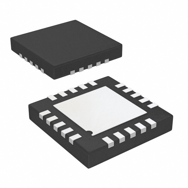
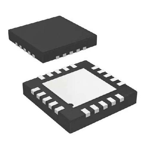
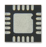
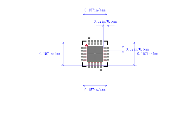
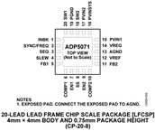
The ADP5071 is available in a 20-lead LFCSP or in a 20-lead TSSOP and is rated for a −40°C to +125°C junction temperature range.
Applications
- .
- Bipolar amplifiers, ADCs, DACs, and multiplexers
- .
- Charge-coupled device CCD bias supply
- .
- Optical module supply
- .
- RF power amplifier PA bias
### Features and Benefits
- .
- Wide input supply voltage range: 2.85 V to 15 V
- .
- Generates well regulated, independently resistor programmable VPOS and VNEG outputs
- .
- Boost regulator to generate VPOS output
- .
- Adjustable positive output to 39 V
- .
- Integrated 2.0 A main switch
- .
- Optional single-ended primary-inductor converter SEPIC configuration for automatic step-up/step-down
- .
- Inverting regulator to generate VNEG output
- .
- Adjustable negative output to VIN − 39 V
- .
- Integrated 1.2 A main switch
- .
- True shutdown for both positive and negative outputs
- .
- 1.2 MHz/2.4 MHz switching frequency with optional external frequency synchronization from 1.0 MHz to 2.6 MHz
- .
- Resistor programmable soft start timer
- .
- Slew rate control for lower system noise
- .
- Individual precision enable and flexible start-up sequence control for symmetric start, VPOS first, or VNEG first
- .
- Out-of-phase operation
- .
- UVLO, OCP, OVP, and TSD protection
- .
- 4 mm × 4 mm, 20-lead LFCSP and 20-lead TSSOP
- .
- −40°C to +125°C junction temperature range
- .
- Supported by the simPower tool set
输出接口数 2
输出电压 2.85V ~ 39V
输出电流 1.2A, 2A
针脚数 20
开关频率 2.4 MHz
输入电压Max 15 V
输入电压Min 2.85 V
工作温度Max 125 ℃
工作温度Min -40 ℃
电源电压Min 2.85 V
输入电压 15 V
安装方式 Surface Mount
引脚数 20
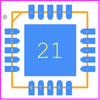
封装 LFCSP-20
高度 0.73 mm
封装 LFCSP-20
工作温度 -40℃ ~ 125℃ TJ
产品生命周期 Active
包装方式 Tray
RoHS标准 RoHS Compliant
含铅标准 Lead Free
REACH SVHC版本 2015/12/17
| 型号/品牌 | 代替类型 | 替代型号对比 |
|---|---|---|
ADP5071ACPZ ADI 亚德诺 | 当前型号 | 当前型号 |
ADP5071ACPZ-R7 亚德诺 | 功能相似 | ADP5071ACPZ和ADP5071ACPZ-R7的区别 |