

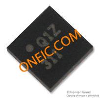
ANALOG DEVICES ADL5565ACPZ-R7 芯片, 射频放大器, 15.5DB, 6GHZ, 5.2V, LFCSP-16
Product Details
The ADL5565 is a high performance differential amplifier optimized for RF and IF applications. The amplifier offers low noise of 1.5 nV/√Hz and excellent distortion performance over a wide frequency range making it an ideal driver for high speed 8-bit to 16-bit analog-to-digital converters ADCs.
The ADL5565 provides three gain levels of 6 dB, 12 dB, and 15.5 dB through a pin strappable configuration. For the single-ended input configuration, the gains are reduced to 5.3 dB, 10.3 dB, and 13 dB. Using two external series resistors expands the gain flexibility of the amplifier and allows for any gain selection from 0 dB to 15.5 dB for a differential input and 0 dB to 13 dB for a single-ended input.
The quiescent current of the ADL5565 is typically 70 mA, and when disabled, consumes less than 5 mA with −25 dB of input-to-output isolation at 100 MHz.
The device is optimized for wideband, low distortion, and noise performance, giving it unprecedented performance for overall spurious-free dynamic range. These attributes, together with its adjustable gain capability, make this device the amplifier of choice for driving a wide variety of ADCs, mixers, pin diode attenuators, SAW filters, and multielement discrete devices.
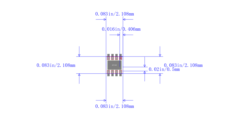
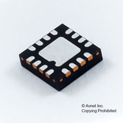
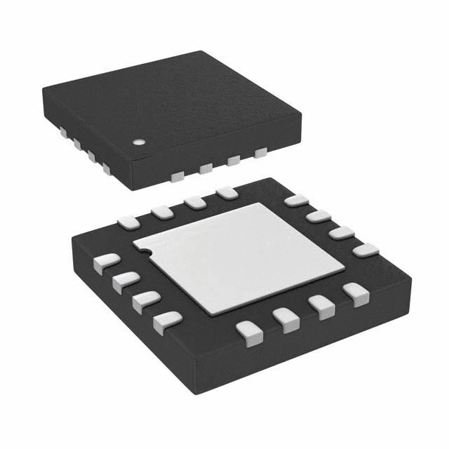
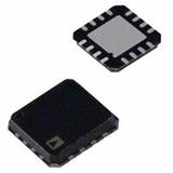
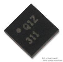
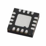
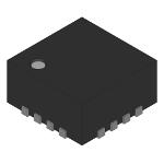
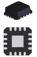
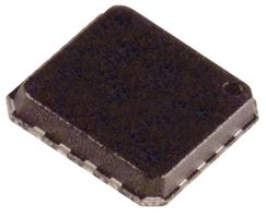
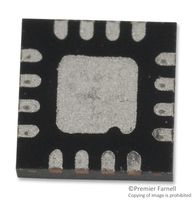
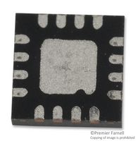
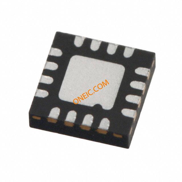
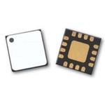
Fabricated on an Analog Devices, Inc., high speed SiGe process, the ADL5565 is supplied in a compact 3 mm × 3 mm, 16-lead LFCSP package and operates over the −40°C to +85°C temperature range.
**Applications**
- .
- Differential ADC drivers
- .
- Single-ended to differential conversion
- .
- RF/IF gain blocks
- .
- SAW filter interfacing
### Features and Benefits
- .
- 3 dB bandwidth of 6 GHz AV = 6 dB
- .
- Pin strappable gain adjust: 6 dB, 12 dB, and 15.5 dB
- .
- Gain range from 0 dB to 15.5 dB using two external resistors
- .
- Differential or single-ended input to differential output
- .
- Low noise input stage: NF = 8.7 dB at 15.5 dB gain
- .
- IMD3 of −112 dBc at 100 MHz center
- .
- Slew rate: 11 V/ns
- .
- Fast settling and overdrive recovery of 2 ns
- .
- Low broadband distortion AV = 6 dB
10 MHz: −107 dBc HD2, −110 dBc HD3
100 MHz: −108 dBc HD2, −103 dBc HD3
200 MHz: −82 dBc HD2,−87 dBc HD3
500 MHz: −68 dBc HD2, −63 dBc HD3
- .
- Single-supply operation: 2.8 V to 5.2 V
- .
- Power down
- .
- Fabricated using the high speed XFCB3 SiGe process
电源电压DC 2.80V min
供电电流 80 mA
电路数 1
通道数 1
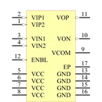
针脚数 16
耗散功率 0.525 W
共模抑制比 60 dB
增益 15.5 dB
输入偏置电流 5 µA
测试频率 100 MHz
工作温度Max 85 ℃
工作温度Min -40 ℃
3dB带宽 7 GHz
耗散功率Max 525 mW
共模抑制比Min 60dB ~ 75dB
电源电压Max 5.2 V
电源电压Min 2.8 V
安装方式 Surface Mount
引脚数 16
封装 LFCSP-16
高度 0.73 mm
封装 LFCSP-16
工作温度 -40℃ ~ 85℃
产品生命周期 Active
包装方式 Tape & Reel TR
制造应用 Aerospace and Defense, Electronic Surveillance and Countermeasures, Radar, Missiles and Precision Munitions
RoHS标准 RoHS Compliant
含铅标准 Contains Lead
REACH SVHC标准 No SVHC
REACH SVHC版本 2015/12/17