可级联IF可变增益放大器 Cascadable IF VGAs
Product Details
The ADL5336 consists of a pair of variable gain amplifiers VGAs designed for cascaded IF applications. The amplifiers have linear-in-dB gain control and operate from low frequencies to 1 GHz. Their excellent gain conformance over the control range and flatness over frequency are due to Analog Devices, Inc., patented X-AMP® architecture, an innovative technique for implementing high performance variable gain control.
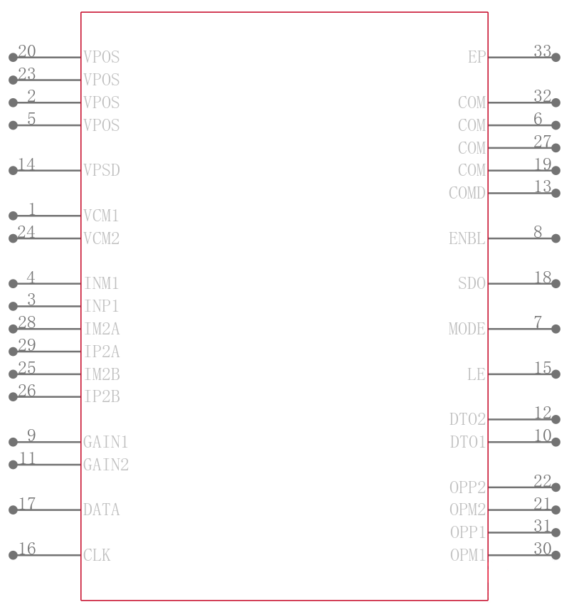
Each VGA has 24 dB of gain control range. Their maximum gain can be independently programmable over a 6 dB range via the SPI. The VGAs can be cascaded to provide a total range of 48 dB. When connected to a 50 Ω source through a 1:4 balun, the gain is 6 dB higher. The second VGA has an SPI programmable input switch that selects one of two external inputs.
When driven from a 200 Ω source or from a 50 Ω source through a 1:4 balun, the noise figure NF for the composite amplifier is 6.8 dB at maximum gain. The output of each VGA can drive 100 Ω loads to 5 V p-p maximum.
Each VGA has an independent square law detector for autonomous, automatic gain control AGC operation. Each detector setpoint can be programmed independently through the SPI from −24 dBV to −3 dBV in 3 dB steps. When both VGAs are arranged in AGC mode and are programmed to the same setpoint, the composite NF increases to 9 dB when backed off by 18 dB from maximum gain.
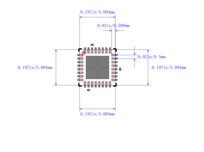
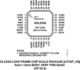
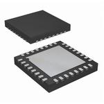
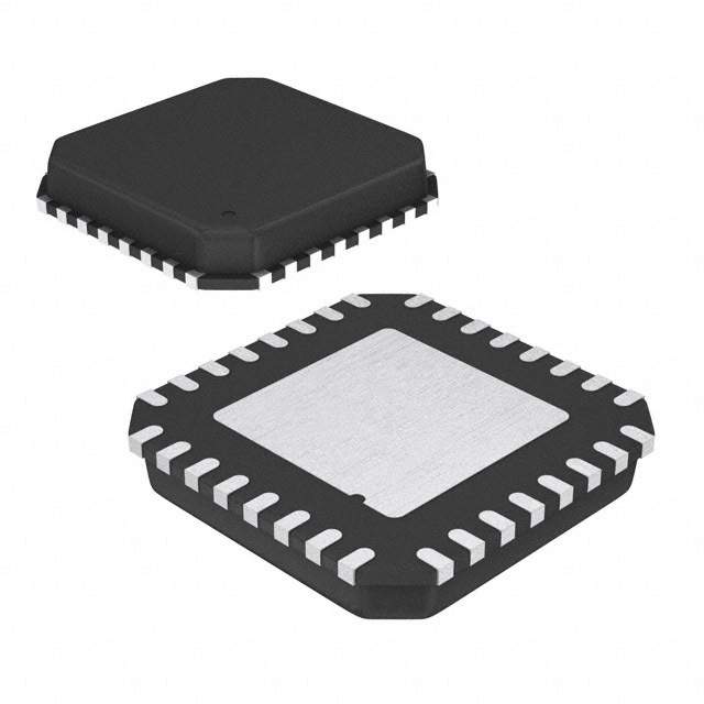
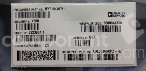
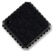
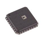
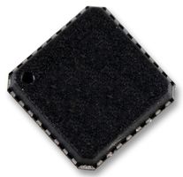
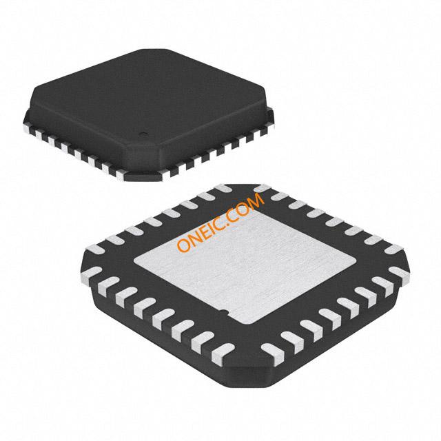
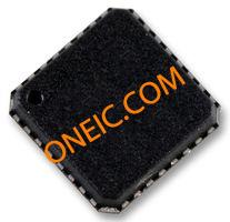
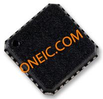
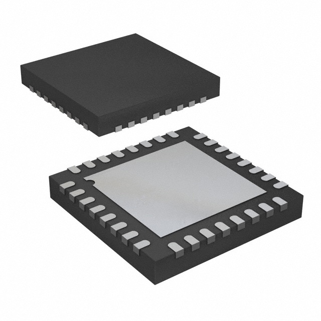
The ADL5336 operates from a 5 V supply and consumes a typical supply current of 80 mA. When disabled, it consumes 4 mA. It is fabricated in an advanced silicon-germanium BiCMOS process and is available in a 32-lead exposed paddle LFCSP package. Performance is specified over a −40°C to +85°C temperature range.
**Applications**
- .
- Point-to-multipoint radios
- .
- Instrumentation
- .
- Medical
### Features and Benefits
- .
- Pair of VGAs with rms AGC detectors
- .
- VGA and AGC modes of operation
- .
- Continuous gain control range: 48 dB
- .
- Noise figure NF = 6.8 dB at maximum gain
- .
- IMD3 > 62 dBc for 1.0 V p-p composite output
- .
- Differential input and output
- .
- Multiplexed inputs for VGA2
- .
- Programmable detector AGC setpoints
- .
- Programmable VGA maximum gain
- .
- Power-down feature
- .
- Single 5 V supply operation
频率 0Hz ~ 1GHz
电源电压DC 4.50V min
供电电流 80 mA
通道数 1
增益 19.5 dB
测试频率 350 MHz
工作温度Max 85 ℃
工作温度Min -40 ℃
电源电压 4.5V ~ 5.5V
电源电压Max 5.5 V
电源电压Min 4.5 V
安装方式 Surface Mount
引脚数 32
封装 LFCSP-32
高度 0.83 mm
封装 LFCSP-32
工作温度 -40℃ ~ 85℃
产品生命周期 Active
包装方式 Tape & Reel TR
RoHS标准 RoHS Compliant
含铅标准 Contains Lead
REACH SVHC标准 No SVHC
REACH SVHC版本 2015/12/17