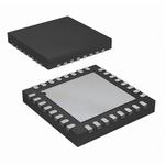

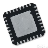
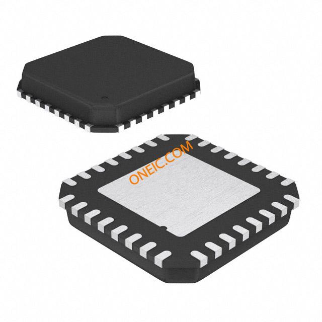
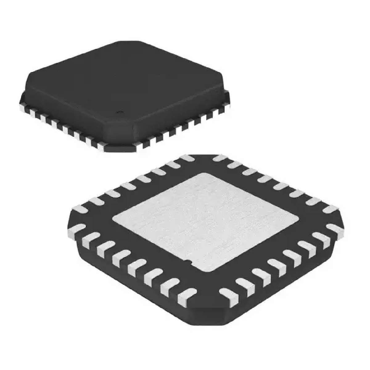
ANALOG DEVICES ADRF6516ACPZ-R7 芯片, 可变增益放大器, 31MHZ, LFCSP-32
Product Details
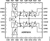
The ADRF6516 is a matched pair of fully differential, low noise and low distortion programmable filters and variable gain amplifiers VGAs. Each channel is capable of rejecting large out-of-band interferers while reliably boosting the desired signal, thus reducing the bandwidth and resolution requirements on the analog-to-digital converters ADCs. The excellent matching between channels and their high spurious-free dynamic range over all gain and bandwidth settings make the ADRF6516 ideal for quadrature-based IQ communication systems with dense constellations, multiple carriers, and nearby interferers.
The filters provide a six-pole Butterworth response with 1 dB corner frequencies programmable through the SPI port from 1 MHz to 31 MHz in 1 MHz steps. The preamplifier that precedes the filters offers a SPI-programmable option of either 3 dB or 6 dB of gain. The preamplifier sets a differential input impedance of 1600 Ω and has a common-mode voltage that defaults to VPS/2 but can be driven from 1.1 V to 1.8 V.
The variable gain amplifiers that follow the filters provide 50 dB of continuous gain control with a slope of 15.5 mV/dB. Their maximum gains can be programmed to various values through the SPI. The output buffers provide a differential output impedance of 30 Ω and are capable of driving 2 V p-p into 1 kΩ loads. The output common-mode voltage defaults to VPS/2, but it can be adjusted down to 700 mV by driving the high impedance VOCM pin. Independent, built-in dc offset compensation loops can be disabled if fully dc-coupled operation is desired. The high-pass corner frequency is defined by external capacitors on the OFS1 and OFS2 pins and the VGA gain.
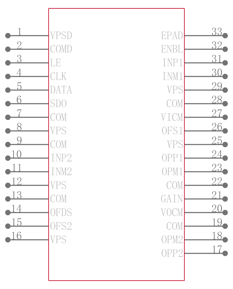
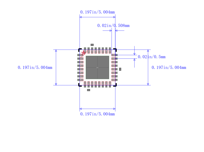
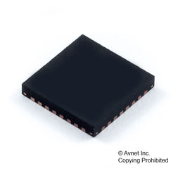
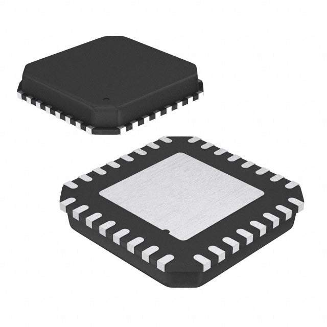
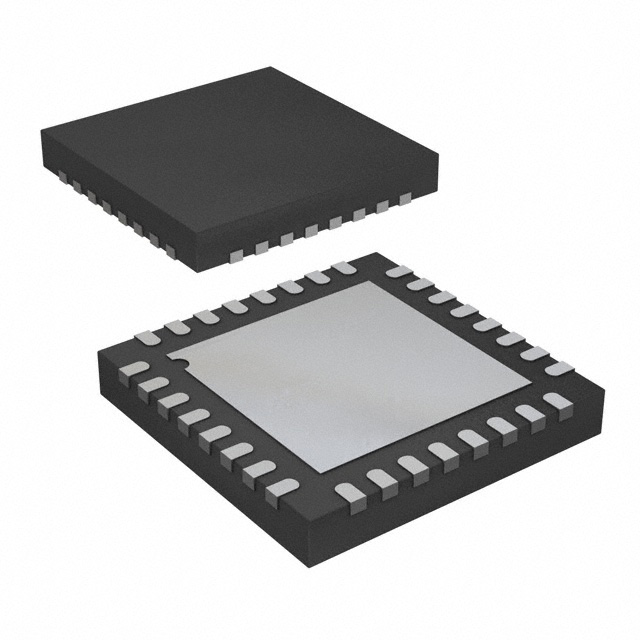
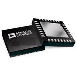
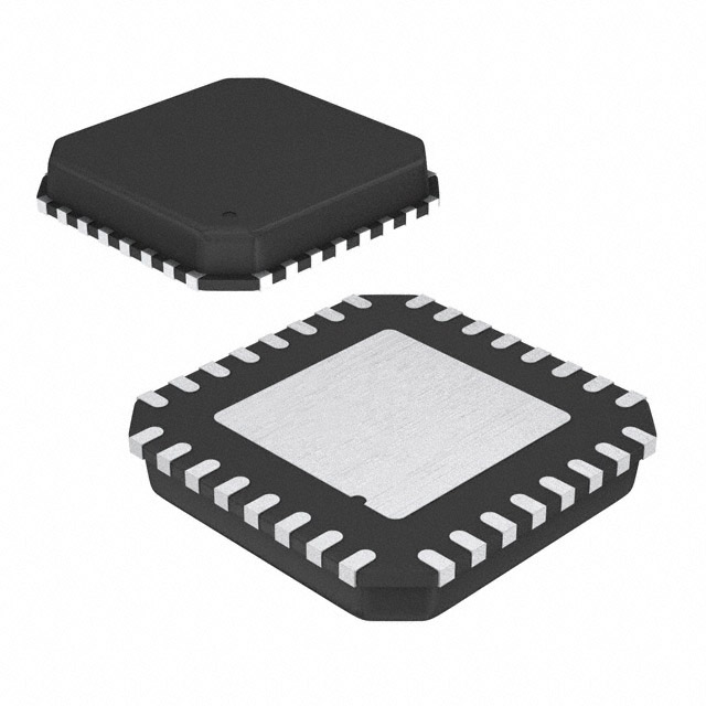
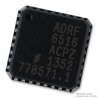
The ADRF6516 operates from a 3.15 V to 3.45 V supply and consumes a maximum supply current of 360 mA when programmed to the highest bandwidth setting. When disabled, it consumes <9 mA. The ADRF6516 is fabricated in an advanced silicon-germanium BiCMOS process and is available in a 32-lead, exposed paddle LFCSP. Performance is specified over the −40°C to +85°C temperature range.
**Applications**
- .
- Baseband I/Q receivers
- .
- Diversity receivers
- .
- ADC drivers
- .
- Point-to-point and point-to-multipoint radio
- .
- Instrumentation
- .
- Medical
### Features and Benefits
- .
- Matched pair of programmable filters and VGAs
- .
- Continuous gain control range: 50 dB
- .
- Digital gain control: 15 dB
- .
- 6-pole Butterworth filter: 1 MHz to 31 MHz in 1 MHz steps, 1 dB corner frequency
- .
- Preamplifier and postamplifier gain steps
- .
- IMD3: >65 dBc for 1.5 V p-p composite output
- .
- HD2, HD3: >65 dBc for 1.5 V p-p output
- .
- Differential input and output
- .
- Flexible output and input common-mode ranges
- .
- Optional dc offset compensation loop
- .
- SPI programmable filter corners and gain steps
- .
- Power-down feature
- .
- Single 3.3 V supply operation