TEXAS INSTRUMENTS CDC3RL02BYFPR 芯片, 时钟扇出缓冲器, 52MHZ, DSBGA-8
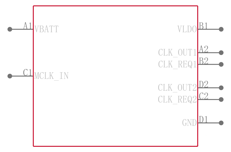
The CDC3RL02 is a two-channel clock fan-out buffer and is ideal for use in portable end-equipment, such as mobile phones, that require clock buffering with minimal additive phase noise and fan-out capabilities. It buffers a single master clock, such as a temperature compensated crystal oscillator TCXO to multiple peripherals. The device has two clock request inputs CLK_REQ1 and CLK_REQ2, each of which enable a single clock output.
The CDC3RL02 accepts square or sine waves at the master clock input MCLK_IN, eliminating the need for an AC coupling capacitor. The smallest acceptable sine wave is a 0.3-V signal peak-to-peak. CDC3RL02 has been designed to offer minimal channel-to-channel skew, additive output jitter, and additive phase noise. The adaptive clock output buffers offer controlled slew-rate over a wide capacitive loading range which minimizes EMI emissions, maintains signal integrity, and minimizes ringing caused by signal reflections on the clock distribution lines.
The CDC3RL02 has an integrated Low-Drop-Out LDO voltage regulator which accepts input voltages from 2.3 V to 5.5 V and outputs 1.8 V, 50 mA. This 1.8-V supply is externally available to provide regulated power to peripheral devices such as a TCXO.
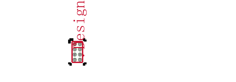
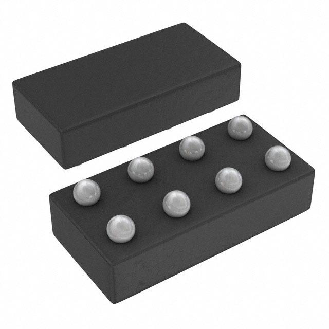
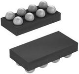
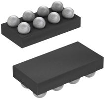
The CDC3RL02 is offered in a 0.4-mm pitch wafer-level chip-scale WCSP package 0.8 mm × 1.6 mm and is optimized for very low standby current consumption.
频率 52 MHz
电源电压DC 2.30V min
输出接口数 2
电路数 1
针脚数 8
占空比 55 %
最大占空比 55 %
工作温度Max 85 ℃
工作温度Min -40 ℃
电源电压 2.3V ~ 5.5V
电源电压Max 5.5 V
电源电压Min 2.3 V
安装方式 Surface Mount
引脚数 8
封装 DSBGA-8
长度 1.59 mm
宽度 0.79 mm
高度 0.5 mm
封装 DSBGA-8
工作温度 -40℃ ~ 85℃
产品生命周期 Active
包装方式 Tape & Reel TR
RoHS标准 RoHS Compliant
含铅标准 Lead Free
REACH SVHC版本 2015/06/15
ECCN代码 EAR99