


C8051F02x Microcontrollers, Silicon LabsThe Silicon Labs C8051F02x are highly integrated mixed-signal microcontrollers MCU with two separate high-speed ADC subsystems. Their two separate 12-bit DACs, on-chip VDD monitor, Watchdog Timer and clock oscillator combine to make the C8051F02x devices standalone System-on-Chip solutions. Enable, disable and configure all the analogue and digital peripherals using the firmware. Flash memory can be reprogrammed even in-circuit, providing non-volatile data storage, and also allowing field upgrades of the 8051 firmware. They are specified for 2.7 V to 3.6 V operation over the industrial temperature range -45°C to +85°C. The C8051F020/2 are available in a 100-pin TQFP package. The C8051F021/3 are available in a 64-pin TQFP package.\- 8051-compatible CIP-51 microcontroller core up to 25 MIPS \- In-system, full-speed, non-intrusive debug interface on-chip \- 12-bit C8051F020/1 or 10-bit C8051F022/3 100 ksps 8-channel ADC with PGA and analogue multiplexer \- 8-bit ADC 500 ksps 8-channel ADC with PGA and analogue multiplexer \- Two 12-bit DACs with programmable update scheduling \- 64 kB of in-system programmable FLASH memory \- 4352 4096 + 256 bytes of on-chip RAM \- External Data Memory Interface with 64 kB address space \- SPI, SMBus/I2C, and two UART serial interfaces implemented in hardware \- 64 digital I/O pins C8051F020/2 or 32 digital I/O pins C8051F021/3 \- Five general purpose 16-bit Timers \- Programmable Counter/Timer Array with five capture/compare modules \- On-chip Watchdog Timer, VDD Monitor, and Temperature Sensor ### 8051 微控制器,Silicon Labs
C8051F02x ,
Silicon Labs C8051F02x 是高度集成的混合信号微控制器 MCU,带两个独立的高速 ADC 子系统。C8051F02x 设备包含两个独立的 12 位 DAC、片上 VDD 监控器、监控计时器和时钟振荡器,是独立的片上系统解决方案。
使用固件启用、禁用和配置所有模拟和数字外围器件。可对闪存进行重新编程(甚至进行在线重新编程),从而提供非易失数据存储,还可现场升级 8051 固件。
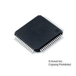
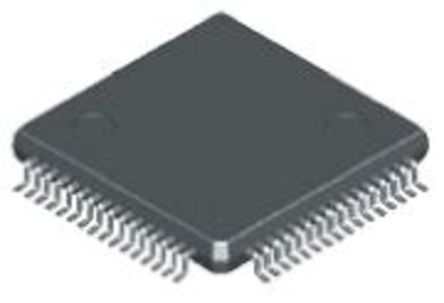
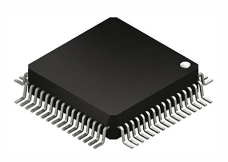
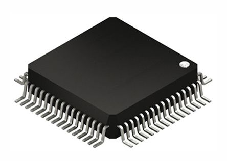
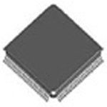
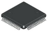
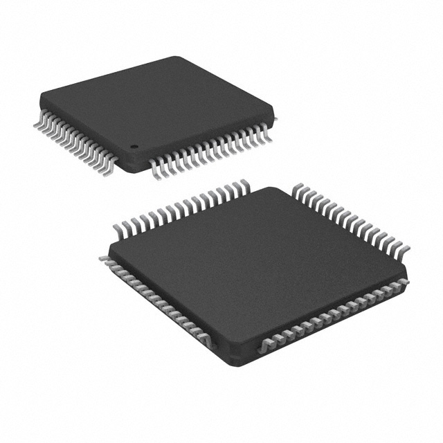
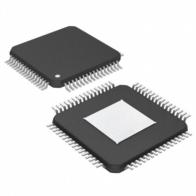
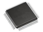
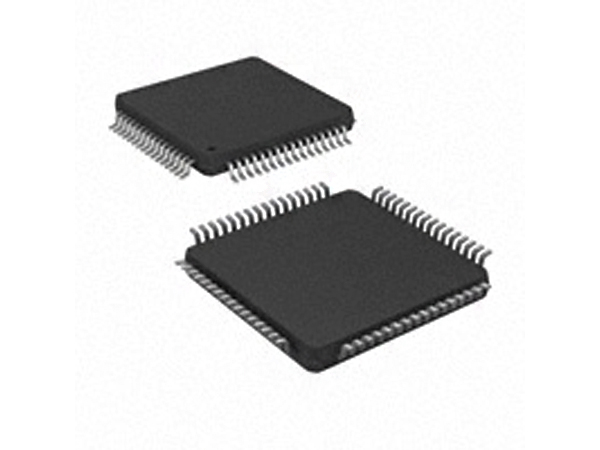
它们指定用于工业温度范围内(45°C 至 +85°C)的 2.7 V 至 3.6 V 操作。C8051F020/2 采用 100 引脚 TQFP 封装。C8051F021/3 提供 64 引脚 TQFP 封装。
\- 8051 兼容的 CIP-51 微控制器核心(高达 25 MIPS)
\- 系统内的全速非侵入式调试接口(片上)
\- 12 C8051F020/1 或 10 位 C8051F022/3 100 ksps 8 通道 ADC,带 PGA 和模拟多路复用器
\- 8 位 ADC 500 ksps 8 通道 ADC,带 PGA 和模拟多路复用器
\- 两个 12 位 DAC,带可编程更新安排
\- 64 kB 的系统内可编程闪存
\- 4352 4096+256 字节的片上 RAM
\- 外部数据存储器接口,带 64 KB 地址空间
\- SPI,SMBus/I2C,和两个在硬件中实施的 UART 串行接口
\- 64 个数字输入/输出引脚 C8051F020/2 或 32 个数字输入/输出引脚 C8051F021/3
\- 五个通用 16 位计时器
\- 可编程计数器/计时器阵列,具有五个捕获/比较模块
\- 片上监控计时器、VDD 监测器和温度传感器
电源电压DC 3.30 V, 3.60 V max
通道数 5
时钟频率 25.0MHz max
RAM大小 4.25K x 8
位数 8
FLASH内存容量 64 KB
I/O引脚数 32
存取时间 25.0 µs
内核架构 8051
模数转换数ADC 1
工作温度Max 85 ℃
工作温度Min -40 ℃
数模转换数DAC 1
电源电压Max 3.6 V
电源电压Min 2.7 V
安装方式 Surface Mount
引脚数 64
封装 TQFP-64
长度 10 mm
宽度 10 mm
高度 1.05 mm
封装 TQFP-64
工作温度 -40℃ ~ 85℃ TA
产品生命周期 Not For New Designs
包装方式 Tray
RoHS标准 RoHS Compliant
含铅标准 Lead Free
| 型号/品牌 | 代替类型 | 替代型号对比 |
|---|---|---|
C8051F023 芯科 | 类似代替 | C8051F023和C8051F023的区别 |
C8051F023-GQR 芯科 | 类似代替 | C8051F023和C8051F023-GQR的区别 |
C8051F023R 芯科 | 类似代替 | C8051F023和C8051F023R的区别 |