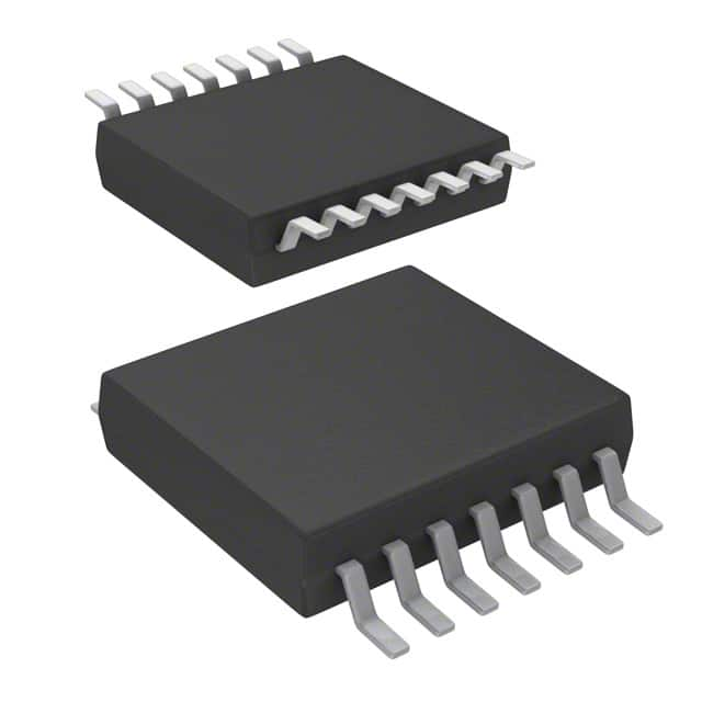


CDCE813QPWRQ1 编带
The CDCE813-Q1 device is a modular Phase-locked-loop-based PLL, low-cost, high-performance, programmable clock synthesizers. They generate up to three output clocks from a single input frequency. Each output can be programmed in-system for any clock frequency up to 230 MHz, using the integrated configurable PLL.
The CDCE813-Q1 has separate output supply pins, VDDOUT, providing 2.5 V to 3.3 V.
The input accepts an external crystal or LVCMOS clock signal. A selectable on-chip VCXO allows synchronization of the output frequency to an external control signal.
The PLL supports SSC spread-spectrum clocking for better electromagnetic interference EMI performance.
The device supports nonvolatile EEPROM programming for easy customization of the device to the application. All device settings are programmable through the I2C bus, a 2-wire serial interface.
The CDCE813-Q1 operates in a 1.8-V core environment as well as eliminating the need for additional, independent XTAL oscillators which reduces component count and board size. It operates in a temperature range of –40°C to 105°C.


