


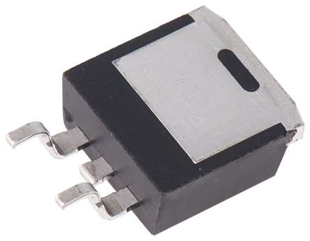
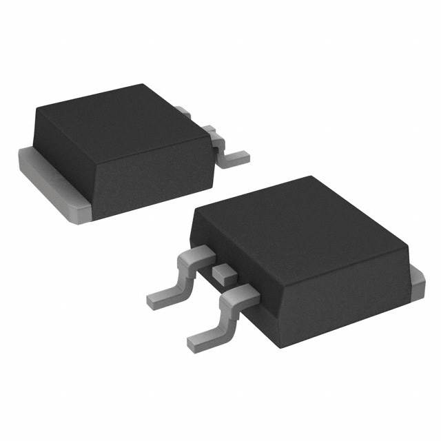
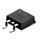


Infineon OptiMOS T 系列 Si N沟道 MOSFET IPB35N10S3L26ATMA1, 35 A, Vds=100 V, 3引脚 D2PAK TO-263封装
OptiMOS™T 功率 MOSFET
OptiMOS™ 产品提供高性能封装,可处理最具挑战性的应用,在有限空间提供全部灵活性。 这些 Infineon 产品经的设计符合并超过计算机应用中更严格的下一代电压调节标准的能效和功率密度要求。
N 通道 - 增强模式
符合汽车 AEC Q101 规格
MSL1 高达 260°C 峰值回流焊接
175°C 工作温度
绿色产品(符合 RoHS 标准)
欧时:
Infineon OptiMOS T 系列 Si N沟道 MOSFET IPB35N10S3L26ATMA1, 35 A, Vds=100 V, 3引脚 D2PAK TO-263封装
得捷:
MOSFET N-CH 100V 35A D2PAK
立创商城:
N沟道 100V 35A
e络盟:
晶体管, MOSFET, N沟道, 35 A, 100 V, 0.0203 ohm, 10 V, 1.7 V
艾睿:
Do you require the advantages of traditional transistors coupled with the switching benefits of power MOSFETs? Infineon Technologies&s; IPB35N10S3L26ATMA1 power MOSFET can provide a solution. Its maximum power dissipation is 71000 mW. In order to guarantee safe delivery and allow for quick mounting of this component after delivery, it will be enclosed in tape and reel packaging during shipment. This device is made with optimos technology. This MOSFET transistor has a minimum operating temperature of -55 °C and a maximum of 175 °C. This N channel MOSFET transistor operates in enhancement mode.
安富利:
Trans MOSFET N-CH 100V 35A 3-Pin2+Tab TO-263
Verical:
Trans MOSFET N-CH 100V 35A Automotive 3-Pin2+Tab D2PAK T/R
Win Source:
MOSFET N-CH TO263-3
针脚数 3
漏源极电阻 0.0203 Ω
极性 N-CH
耗散功率 71 W
阈值电压 1.7 V
漏源极电压Vds 100 V
连续漏极电流Ids 35A
上升时间 4 ns
输入电容Ciss 2070pF @25VVds
下降时间 3 ns
工作温度Max 175 ℃
工作温度Min -55 ℃
耗散功率Max 71W Tc
安装方式 Surface Mount
引脚数 3
封装 TO-263-3
长度 10.31 mm
宽度 9.45 mm
高度 4.57 mm
封装 TO-263-3
工作温度 -55℃ ~ 175℃
产品生命周期 Active
包装方式 Tape & Reel TR
制造应用 48V DC/DC, 48V inverter, HID lighting
RoHS标准
含铅标准 Lead Free