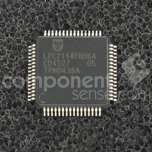
NXP恩智浦/LPC2114FBD64
General description
The LPC2114/2124 are based on a 16/32-bit ARM7TDMI-S CPU with real-time emulation and embedded trace support, together with 128/256 kB of embedded high-speed flash memory. A 128-bit wide memory interface and a unique accelerator architecture enable 32-bit code execution at maximum clock rate. For critical code size applications, the alternative 16-bit Thumb mode reduces code by more than 30 % with minimal performance penalty.
Features and benefits
Key features brought by LPC2114/2124/01 devices
■ Fast GPIO ports enable port pin toggling up to 3.5 times faster than the original device. They also allow for a port pin to be read at any time regardless of its function.
■ Dedicated result registers for ADCs reduce interrupt overhead. The ADC pads are 5 V tolerant when configured for digital I/O functions.
■ UART0/1 include fractional baud rate generator, auto-bauding capabilities and handshake flow-control fully implemented in hardware.
■ Buffered SSP serial controller supporting SPI, 4-wire SSI, and Microwire formats.
■ SPI programmable data length and master mode enhancement.
■ Diversified Code Read Protection CRP enables different security levels to be implemented. This feature is available in LPC2114/2124/00 devices as well.
■ General purpose timers can operate as external event counters.
Key features common for all devices
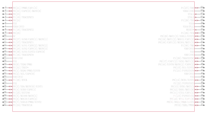
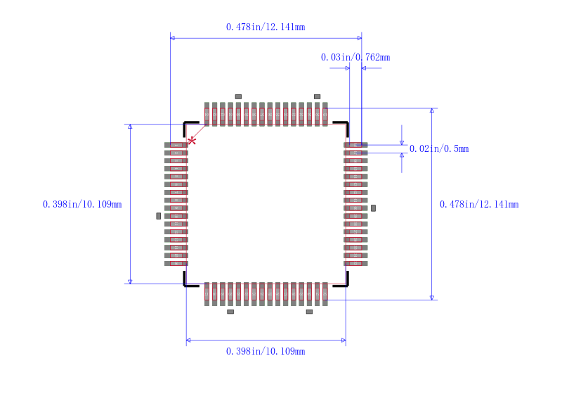
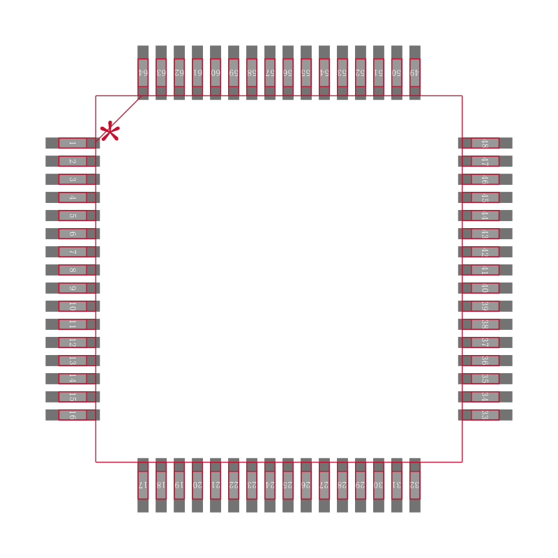
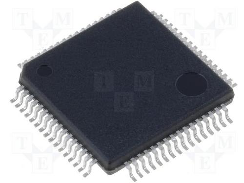
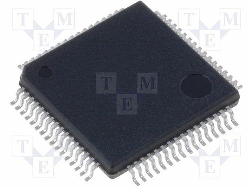
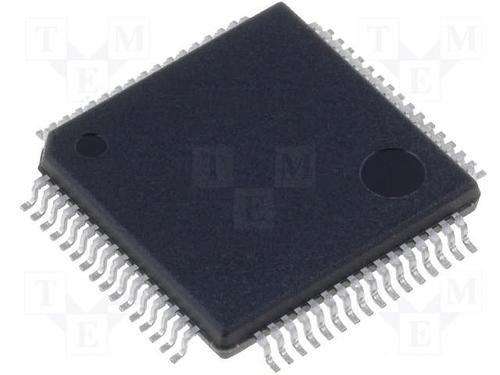
■ 16/32-bit ARM7TDMI-S microcontroller in a tiny LQFP64 package.
■ 16 kB on-chip static RAM.
■ 128/256 kB on-chip flash program memory. 128-bit wide interface/accelerator enables high speed 60 MHz operation.
■ In-System Programming ISP and In-Application Programming IAP via on-chip bootloader software. Flash programming takes 1 ms per 512 B line. Single sector or full chip erase takes 400 ms.
■ EmbeddedICE-RT interface enables breakpoints and watch points. Interrupt service routines can continue to execute whilst the foreground task is debugged with the on-chip RealMonitor software.
■ Embedded Trace Macrocell ETM enables non-intrusive high speed real-time tracing of instruction execution.
■ Four-channel 10-bit ADC with conversion time as low as 2.44 s.
■ Two 32-bit timers with four capture and four compare channels, PWM unit six outputs, Real-Time Clock RTC and watchdog.
■ Multiple serial interfaces including two UARTs 16C550, Fast I2C-bus 400 kbit/s and two SPIs.
■ 60 MHz maximum CPU clock available from programmable on-chip Phase-Locked Loop with settling time of 100s.
■ Vectored Interrupt Controller with configurable priorities and vector addresses.
■ Up to forty-six 5 V tolerant general purpose I/O pins. Up to nine edge or level sensitive external interrupt pins available.
■ On-chip crystal oscillator with an operating range of 1 MHz to 30 MHz.
■ Two low power modes, Idle and Power-down.
■ Processor wake-up from Power-down mode via external interrupt.
■ Individual enable/disable of peripheral functions for power optimization.
■ Dual power supply:
♦ CPU operating voltage range of 1.65 V to 1.95 V 1.8 V ± 0.15 V.
♦ I/O power supply range of 3.0 V to 3.6 V 3.3 V ± 10 % with 5 V tolerant I/O pads. 16/32-bit ARM7TDMI-S processor.