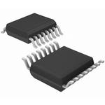
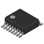


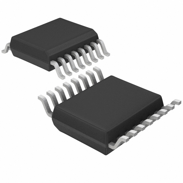
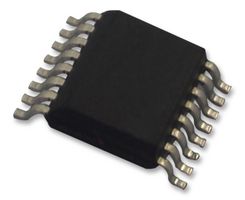
LINEAR TECHNOLOGY LTC6082CGN#PBF 运算放大器, 四路, 3.6 MHz, 4个放大器, 1 V/µs, 2.7V 至 5.5V, SSOP, 16 引脚
The is a quad low offset/drift/noise CMOS Operational Amplifier with rail-to-rail input/output swing. The 70µV maximum offset, 1pA input bias current, 120dB open loop gain and 1.3µVP-P 0.1Hz to 10Hz noise make it perfect for precision signal conditioning. The LTC6082 features 100dB CMRR and 98dB PSRR. Each amplifier consumes only 330µA of current on a 3V supply. The 10-lead DFN has an independent shutdown function that reduces each amplifier"s supply current to 1µA. LTC6082 is specified for power supply voltages of 3 and 5V from -40 to 125°C.
- .
- 0.8µV/°C Maximum offset drift
- .
- 120dB Typical open loop voltage gain
- .
- Unity-gain stable
供电电流 340 µA
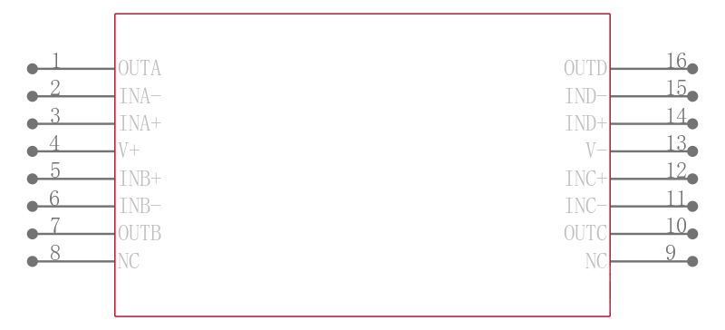
电路数 4
针脚数 16
带宽 3.6 MHz
转换速率 1.00 V/μs
增益频宽积 3.5 MHz
输入补偿电压 70 µV
输入偏置电流 0.2 pA
工作温度Max 85 ℃
工作温度Min -40 ℃
增益带宽 3.5 MHz
共模抑制比Min 100 dB
电源电压 2.7V ~ 5.5V
电源电压Max 5.5 V
安装方式 Surface Mount
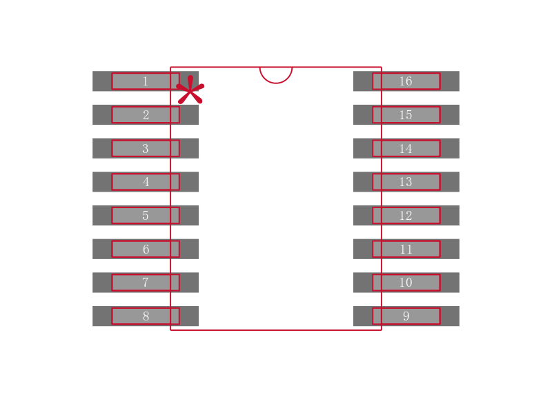
引脚数 16
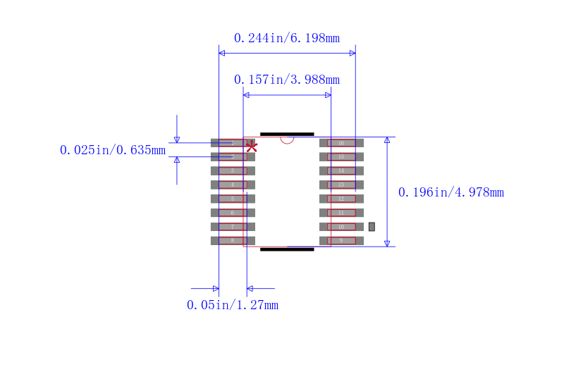
封装 SSOP-16
高度 1.5 mm
封装 SSOP-16
工作温度 0℃ ~ 70℃
产品生命周期 Unknown
包装方式 Each
制造应用 传感与仪器, 信号处理, Signal Processing, Sensing & Instrumentation
RoHS标准 RoHS Compliant
含铅标准 Lead Free
REACH SVHC标准 No SVHC
REACH SVHC版本 2015/12/17
| 型号/品牌 | 代替类型 | 替代型号对比 |
|---|---|---|
LTC6082CGN#PBF Linear Technology 凌力尔特 | 当前型号 | 当前型号 |
LTC6082IGN#PBF 凌力尔特 | 完全替代 | LTC6082CGN#PBF和LTC6082IGN#PBF的区别 |
LTC6082CGN#TRPBF 凌力尔特 | 完全替代 | LTC6082CGN#PBF和LTC6082CGN#TRPBF的区别 |