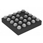
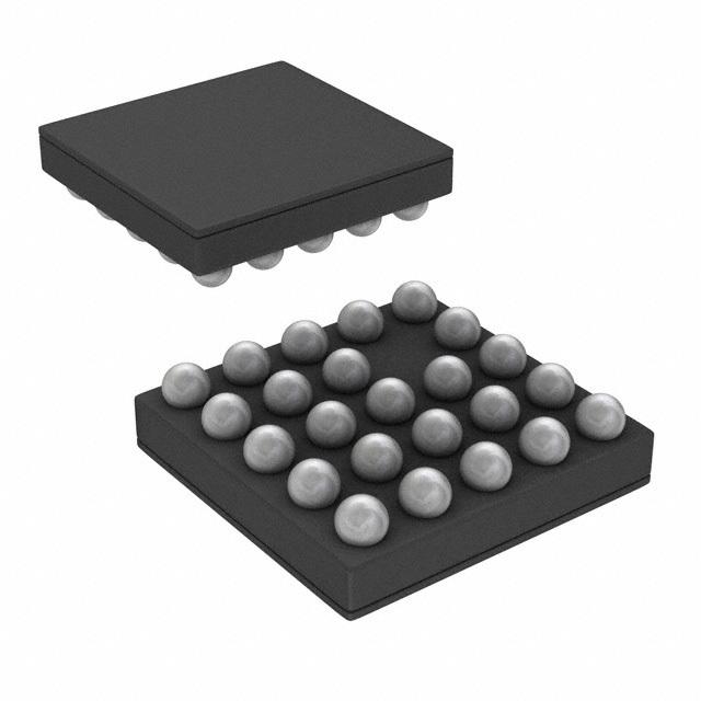
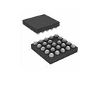
High Speed Bi-Directional Level Shifter & Ultra Low-Dropout CMOS Voltage Regulator & Line Protection 24-DSBGA
The LP3929 is designed for portable and wireless applications requiring level translation and power supply generation in a compact footprint.
The device level translates 1.8 V LVCMOS on the host A side to 2.85 V LVCMOS levels on the card B side for a miniSD / SD 4-bit bi-directional data bus.
Independent direct control of the CMD, Data0 and Data1-3 paths support mini SD state machine requirements. A shutdown pin is provided for the level shifters and regulator. The f_CLK_A is a feedback clock to the host which can be used to overcome level shifter bus delay.
The built-in low-dropout voltage regulator is ideal for mobile phone and battery powered wireless applications. It provides up to 200 mA from a 3.05 V to 5.5 V input. It is stable with small 1.0 µF ±30% ceramic and high quality tantalum output capacitors, requiring smallest possible PC board area.
The card B port side channels have integration of ASIP Application Specific Integrated Passives - on chip integrated pull-up, pull-down, series resistors and capacitors for EMC filtering. It is designed to tolerate IEC61000-4-2 level 4 ESD: ±15 kV air discharge, ±8 kV direct contact.