


MC74HC367ADTG概述
MC74HC367A: 六路 3 态非反相缓冲器,带单独的 2 位和 4 位分区
The MC74HC367A is identical in pinout to the LS367. The device inputs are compatible with standard CMOS outputs; with pullup resistors, they are compatible with LSTTL outputs. This device is arranged into 2-bit and 4-bit sections, each having its own active-low Output Enable. When either of the enables is high, the affected buffer outputs are placed into high-impedance states. The HC367A has noninverting outputs.
Features
---
|
- .
- Output Drive Capability: 15 LSTTL Loads
- .
- Outputs Directly Interface to CMOS, NMOS, and TTL
- .
- Operating Voltage Range: 2 to 6 V
- .
- Low Input Current: 1 mA
- .
- High Noise Immunity Characteristic of CMOS Devices
- .
- In Compliance with the Requirements Defined by JEDEC Standard No. 7A
- .
- Chip Complexity: 92 FETs or 23 Equivalent Gates
MC74HC367ADTG中文资料参数规格
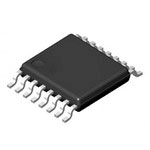
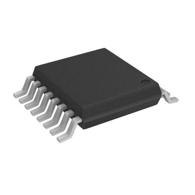
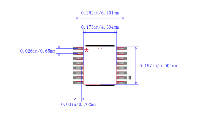
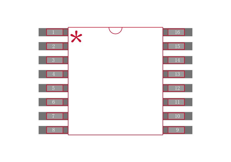
MC74HC367ADTG引脚图与封装图 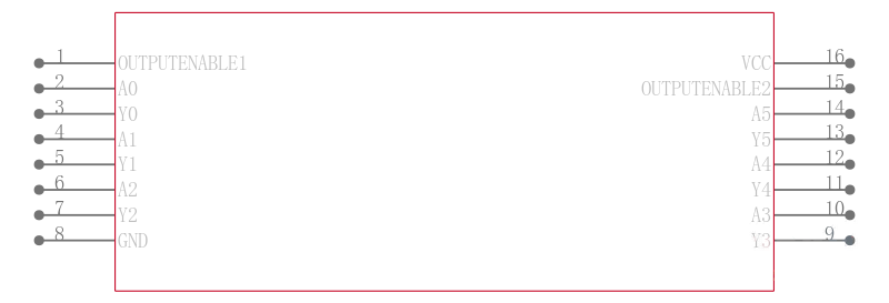
在线购买MC74HC367ADTG