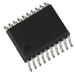


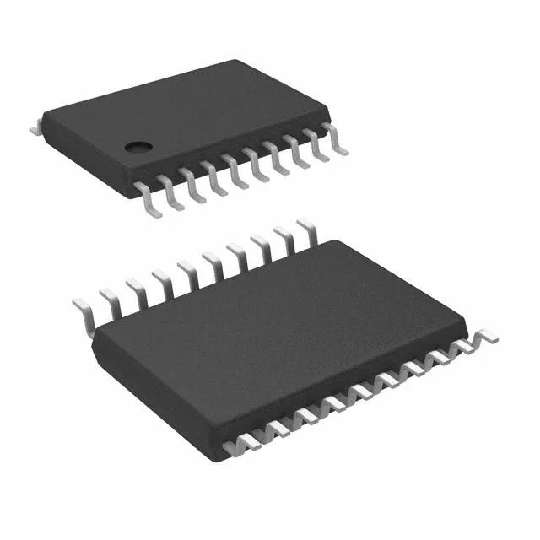


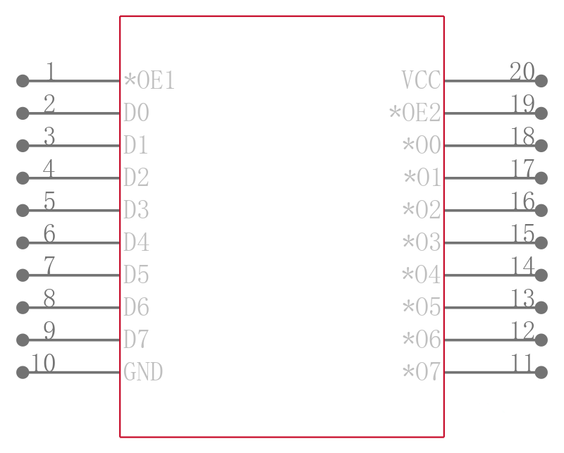
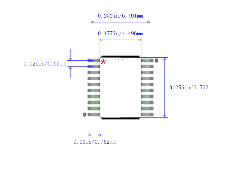
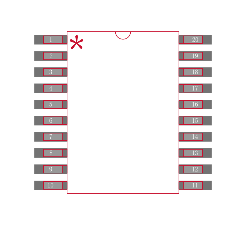
低电压CMOS八路缓冲器流量引脚排列 Low-Voltage CMOS Octal Buffer Flow Through Pinout
By driving the input to the transmission line this buffer and line driver by will amplify any signal. With a 3-state output, this is power management at its best. This line driver has an operating temperature range of -40 °C to 85 °C. In order to ensure safe delivery and enable quick mounting of this component after delivery, it will be encased in tape and reel packaging during shipment. It has 8 channels per chip. This inverting device has a typical operating supply voltage of 3.3 V. Its minimum operating supply voltage of 2 V, while its maximum is 3.6 V.
| 型号/品牌 | 代替类型 | 替代型号对比 |
|---|---|---|
MC74LCX540DTR2G ON Semiconductor 安森美 | 当前型号 | 当前型号 |
74LCX540MTC 安森美 | 完全替代 | MC74LCX540DTR2G和74LCX540MTC的区别 |
SN74LVC540ADW 德州仪器 | 功能相似 | MC74LCX540DTR2G和SN74LVC540ADW的区别 |
SN74LVC540APW 德州仪器 | 功能相似 | MC74LCX540DTR2G和SN74LVC540APW的区别 |