


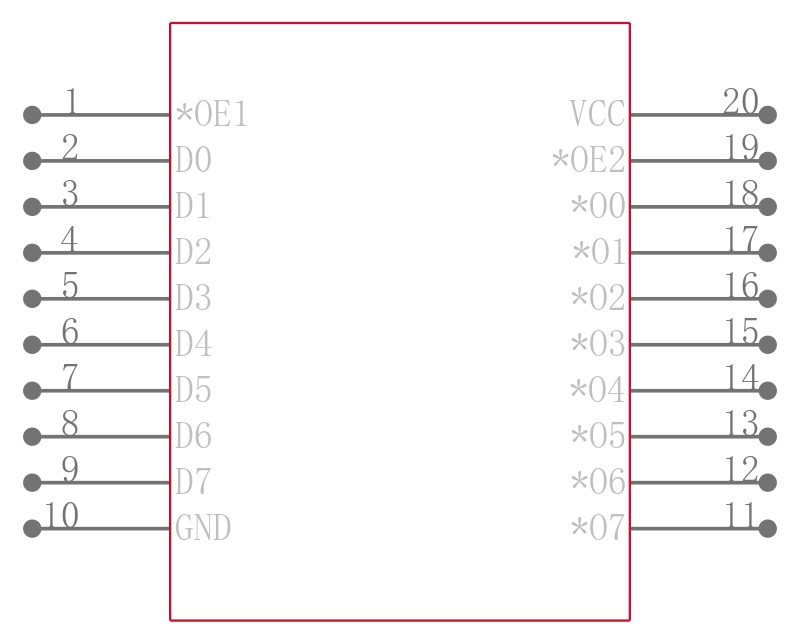
低电压CMOS八路缓冲器流量引脚排列 Low-Voltage CMOS Octal Buffer Flow Through Pinout
Leading the input to the transmission line this buffer and line driver by will amplify digital and analog signals. With a 3-state output, this is power management at its best. This line driver has an operating temperature range of -40 °C to 85 °C. Tape and reel packaging will encase the product during shipment, ensuring safe delivery and enabling quick mounting of components. This inverting device has a typical operating supply voltage of 3.3 V. Its minimum operating supply voltage of 2 V, while its maximum is 3.6 V. It has 8 channels per chip.
电源电压DC 3.60V max
无卤素状态 Halogen Free
输出接口数 8
电路数 1
通道数 8
位数 8
输入数 8
工作温度Max 85 ℃
工作温度Min -40 ℃
电源电压 2V ~ 3.6V
电源电压Max 3.6 V
电源电压Min 2 V
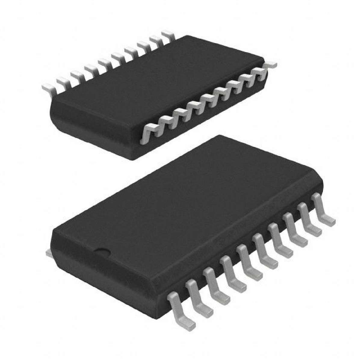
安装方式 Surface Mount
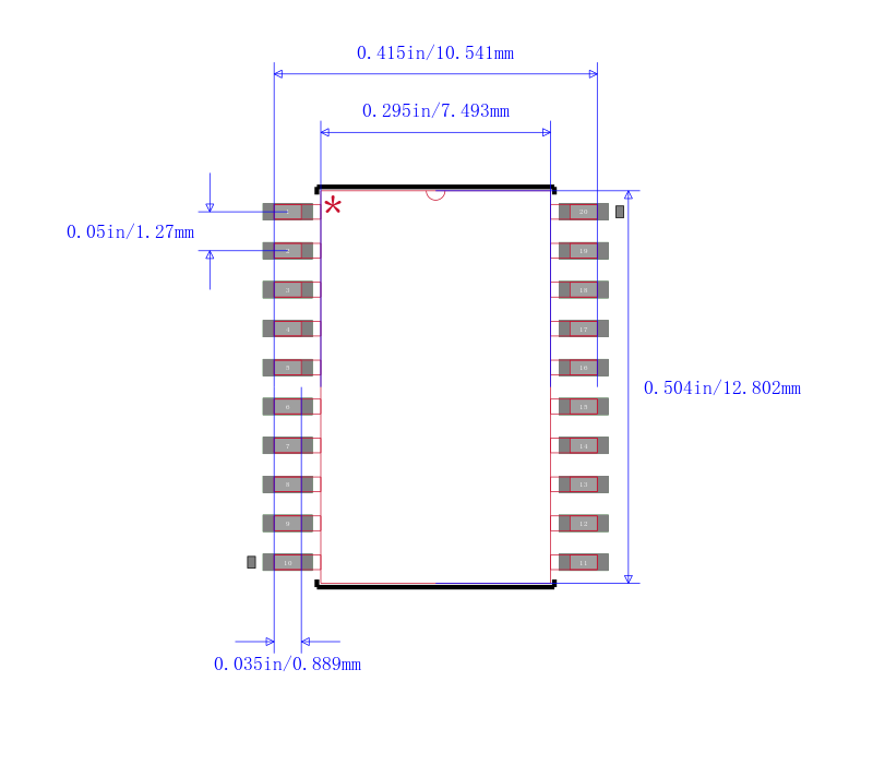
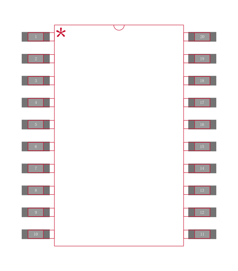
引脚数 20
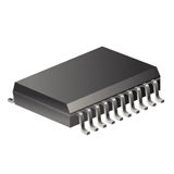
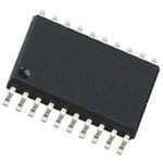
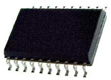
封装 SOIC-20
封装 SOIC-20
工作温度 -40℃ ~ 85℃ TA
产品生命周期 Active
包装方式 Tape & Reel TR
RoHS标准 RoHS Compliant
含铅标准 Lead Free
ECCN代码 EAR99
| 型号/品牌 | 代替类型 | 替代型号对比 |
|---|---|---|
MC74LCX540DWR2G ON Semiconductor 安森美 | 当前型号 | 当前型号 |
MC74LCX540DWR2 安森美 | 完全替代 | MC74LCX540DWR2G和MC74LCX540DWR2的区别 |