


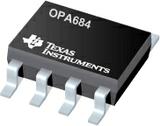


低功耗,电流反馈运算放大器,具有禁用 Low-Power, Current Feedback OPERATIONAL AMPLIFIER With Disable
The OPA684 provides a new level of performance in low-power, wideband, current-feedback CFB amplifiers. This CFB_plus_ amplifier is the first to use an internally closed-loop input buffer stage that enhances performance significantly over earlier low-power CFB amplifiers. While retaining the benefits of very low power operation, this new architecture provides many of the benefits of a more ideal CFB amplifier. The closed-loop input stage buffer gives a very low and linearized impedance path at the inverting input to sense the feedback error current. This improved inverting input impedance retains exceptional bandwidth to much higher gains and improves harmonic distortion over earlier solutions limited by inverting input linearity. Beyond simple high-gain applications, the OPA684 CFB_plus_ amplifier permits the gain setting element to be set with considerable freedom from amplifier bandwidth interaction. This allows frequency response peaking elements to be added, multiple input inverting summing circuits to have greater bandwidth, and low-power line drivers to meet the demanding requirements of studio cameras and broadcast video.
The output capability of the OPA684 also sets a new mark in performance for low-power current feedback amplifiers. Delivering a full ±4Vpp swing on ±5V supplies, the OPA684 also has the output current to support this swing into a 100 load. This minimal output headroom requirement is complemented by a similar 1.2V input stage headroom giving exceptional capability for single +5V operation.
The OPA684s low 1.7mA supply current is precisely trimmed at 25°C. This trim, along with low shift over temperature and supply voltage, gives a very robust design over a wide range of operating conditions. System power may be further reduced by using the optional disable control pin. Leaving this disable pin open, or holding it HIGH, gives normal operation. If pulled LOW, the OPA684 supply current drops to less than 100µA while the I/O pins go to a high impedance state.
输出电流 80mA @5V
供电电流 1.7 mA
电路数 1
通道数 1
共模抑制比 52 dB
输入补偿漂移 12.0 µV/K
带宽 210 MHz
转换速率 820 V/μs
增益频宽积 210 MHz
输入补偿电压 1.5 mV
输入偏置电流 5 µA
可用通道 S, D, Q, T
工作温度Max 85 ℃
工作温度Min -40 ℃
3dB带宽 210 MHz
增益带宽 1.9 GHz
共模抑制比Min 52 dB
安装方式 Surface Mount
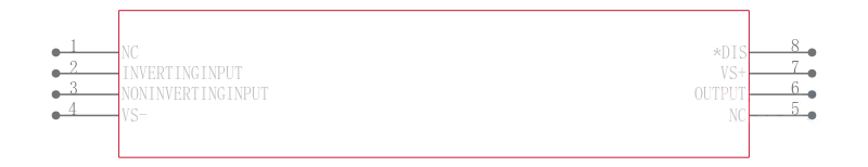
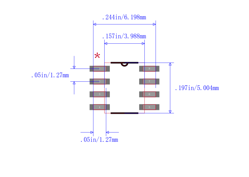
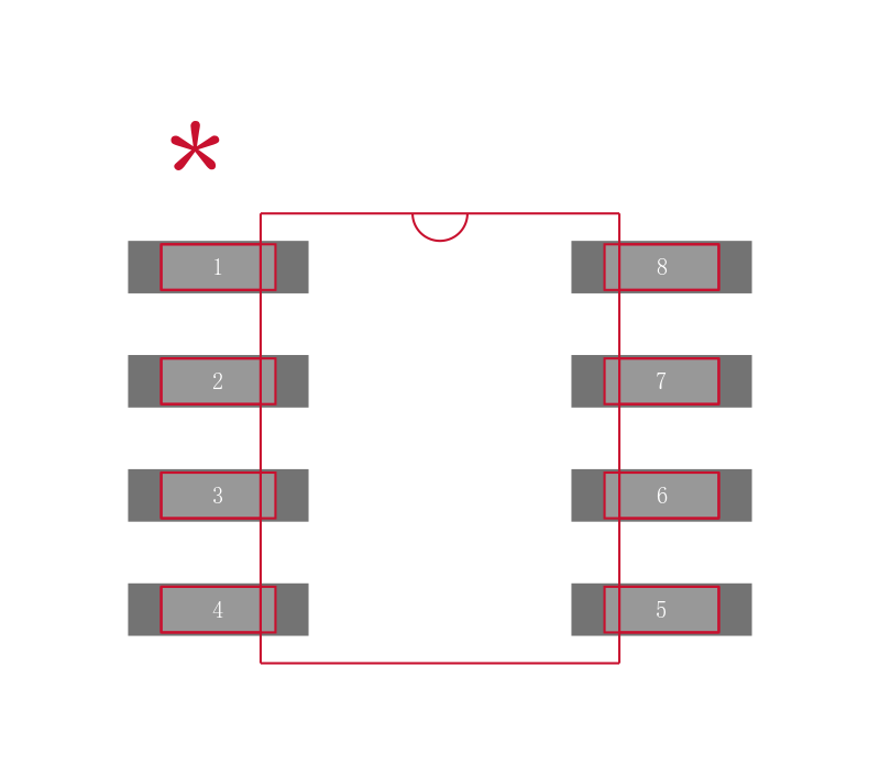
引脚数 8
封装 SOIC-8
长度 4.9 mm
宽度 3.91 mm
高度 1.58 mm
封装 SOIC-8
工作温度 -40℃ ~ 85℃
产品生命周期 Active
包装方式 Tube
RoHS标准 RoHS Compliant
含铅标准 Lead Free
REACH SVHC标准 No SVHC
REACH SVHC版本 2015/06/15
| 型号/品牌 | 代替类型 | 替代型号对比 |
|---|---|---|
OPA684ID TI 德州仪器 | 当前型号 | 当前型号 |
OPA684IDR 德州仪器 | 类似代替 | OPA684ID和OPA684IDR的区别 |
OPA684IDG4 德州仪器 | 类似代替 | OPA684ID和OPA684IDG4的区别 |
OPA684IDRG4 德州仪器 | 类似代替 | OPA684ID和OPA684IDRG4的区别 |