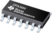

具有禁用功能的低功耗三路电流反馈运算放大器
The provides a new level of performance in low-power, wideband, current-feedback CFB amplifiers. This CFB_PLUS_ amplifier among the first to use an internally closed-loop input buffer stage that enhances performance significantly over earlier low-power CFB amplifiers. While retaining the benefits of very low power operation, this new architecture provides many of the benefits of a more ideal CFB amplifier. The closed-loop input stage buffer gives a very low and linearized impedance path at the inverting input to sense the feedback error current. This improved inverting input impedance retains exceptional bandwidth to much higher gains and improves harmonic distortion over earlier solutions limited by inverting input linearity. Beyond simple high-gain applications, the OPA3684 CFB_PLUS_ amplifier permits the gain setting element to be set with considerable freedom from amplifier bandwidth interaction. This allows frequency response peaking elements to be added, multiple input inverting summing circuits to have greater bandwidth, and low-power line drivers to meet the demanding requirements of studio cameras and broadcast video. The output capability of the OPA3684 also sets a new mark in performance for low-power current-feedback amplifiers. Delivering a full ±4Vp-p swing on ±5V supplies, the OPA3684 also has the output current to support > ±3Vp-p into 50. This minimal output headroom requirement is complemented by a similar 1.2V input stage headroom giving exceptional capability for single +5V operation.
The OPA3684s low 1.7mA/ch supply current is precisely trimmed at 25°C. This trim, along with low shift over temperature and supply voltage, gives a very robust design over a wide range of operating conditions. System power may be further reduced by using the optional disable control pin. Leaving this disable pin open, or holding it HIGH, gives normal operation. If pulled LOW, the OPA3684 supply current drops to less than 100µA/ch while the I/O pins go to a high impedance state.
- .
- MINIMAL BANDWIDTH CHANGE VERSUS GAIN
- .
- 170MHz BANDWIDTH: G = +2
- .
- > 120MHz BANDWIDTH TO GAIN > +10
- .
- LOW DISTOR ON: < 82dBc at 5MHz
- .
- HIGH OUTPUT CURRENT: 120mA
- .
- SINGLE +5V TO +12V SUPPLY OPERATION
- .
- DUAL ±.5V TO ±6.0V SUPPLY OPERATION
- .
- LOW SUPPLY CURRENT: 1.7mA/ch
- .
- LOW SHUTDOWN CURRENT: 100µA/ch
- .
- APPLICATIONS
- .
- RGB LINE DRIVERS
- .
- LOWPOWER BROADCAST VIDEO DRIVERS
- .
- EQUALIZING FILTERS
- .
- MULTICHANNEL SUMMING AMPLIFIERS
- .
- PROFESSIONAL CAMERAS
- .
- ADC INPUT DRIVERS
All trademarks are the property of their respective owners.
| 型号/品牌 | 代替类型 | 替代型号对比 |
|---|---|---|
OPA3684 TI 德州仪器 | 当前型号 | 当前型号 |
OPA684 德州仪器 | 功能相似 | OPA3684和OPA684的区别 |