
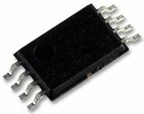

NXP PCA9306DP 芯片, 电压转换器, I2C/SMBUS, 8TSSOP
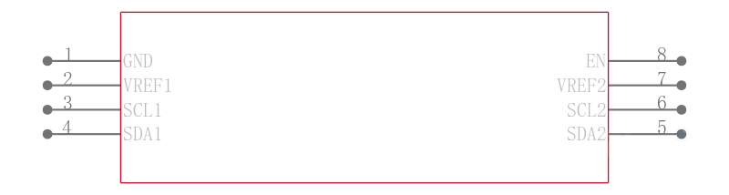
The is a dual bidirectional I²C-bus and SMBus Voltage-level Translator with an enable EN input and is operational from 1 to 3.6V Vref1 and 1.8 to 5.5V Vbiasref2. It allows bidirectional voltage translations between 1 and 5V without the use of a direction pin. The low ON-state resistance Ron of the switch allows connections to be made with minimal propagation delay. When EN is high, the translator switch is on and the SCL1 and SDA1 I/O are connected to the SCL2 and SDA2 I/O, respectively, allowing bidirectional data flow between ports. When EN is low, the translator switch is off and a high-impedance state exists between ports. The PCA9306 is not a bus buffer like the PCA9509 or PCA9517A that provide both level translation and physically isolates the capacitance to either side of the bus when both sides are connected. The PCA9306 only isolates both sides when the device is disabled and provides voltage level translation when active.
- .
- 2-bit Bidirectional translator for SDA and SCL lines in mixed-mode I²C-bus applications
- .
- Standard-mode, fast-mode and fast-mode plus I²C-bus and SMBus compatible
- .
- Low 3.5W ON-state connection between input and output ports
- .
- High-impedance SCL1, SDA1, SCL2 and SDA2 pins for EN = low
- .
- Lock-up free operation
- .
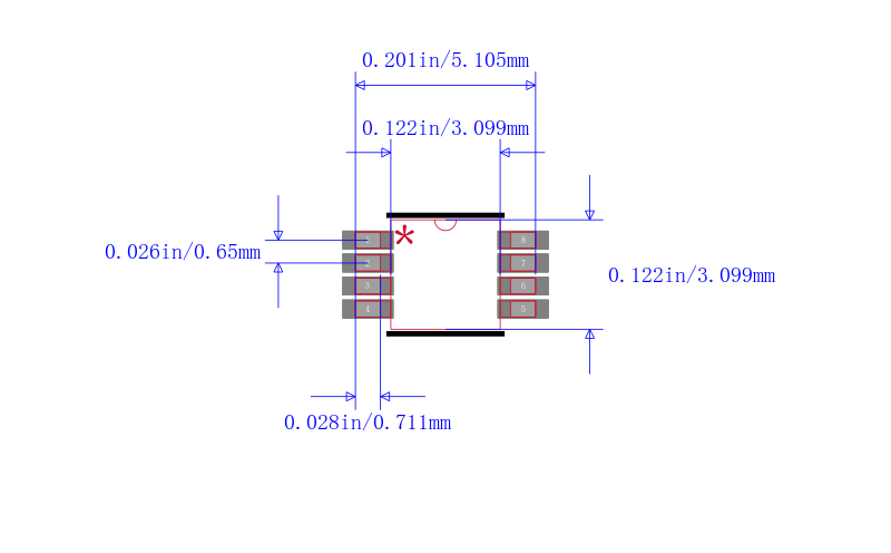
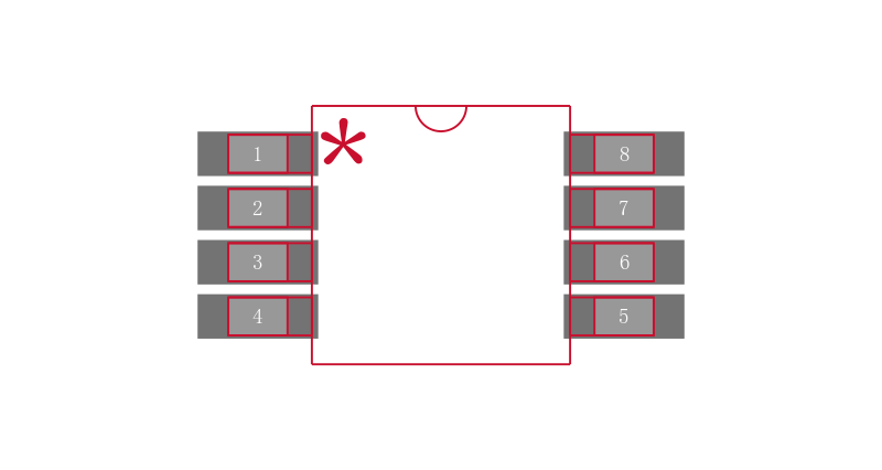
- Flow through pinout for ease of printed-circuit board trace routing