

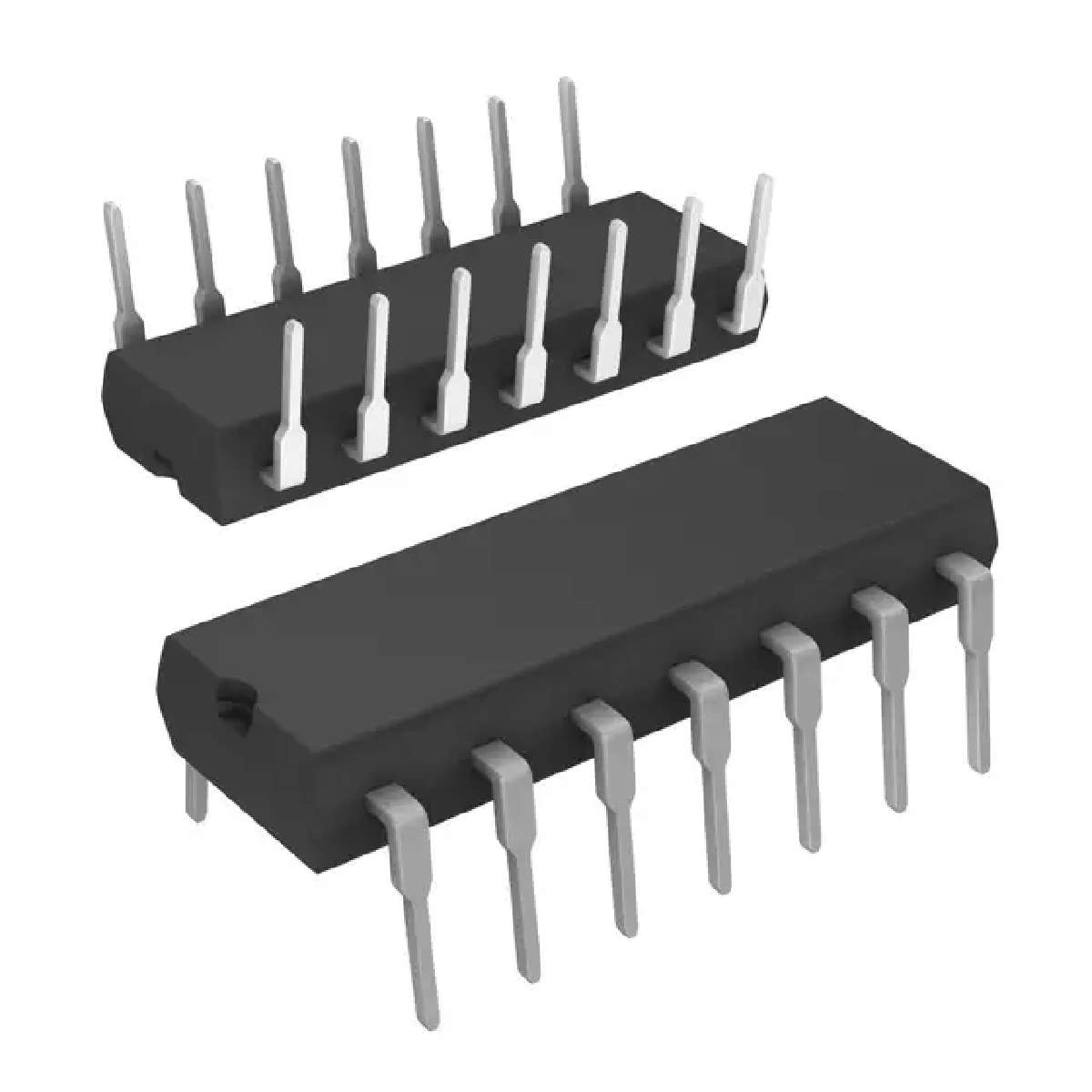
MCU 8Bit PIC16 PIC RISC 3.5KB Flash 3.3V/5V Automotive 14Pin PDIP Tube
DEVICE OVERVIEW
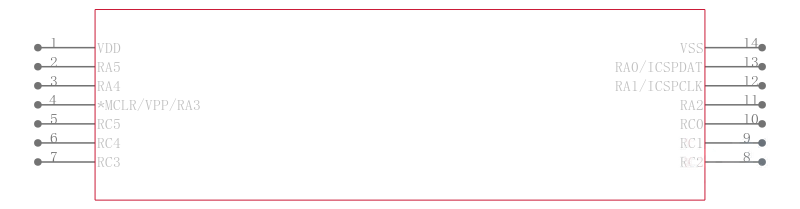
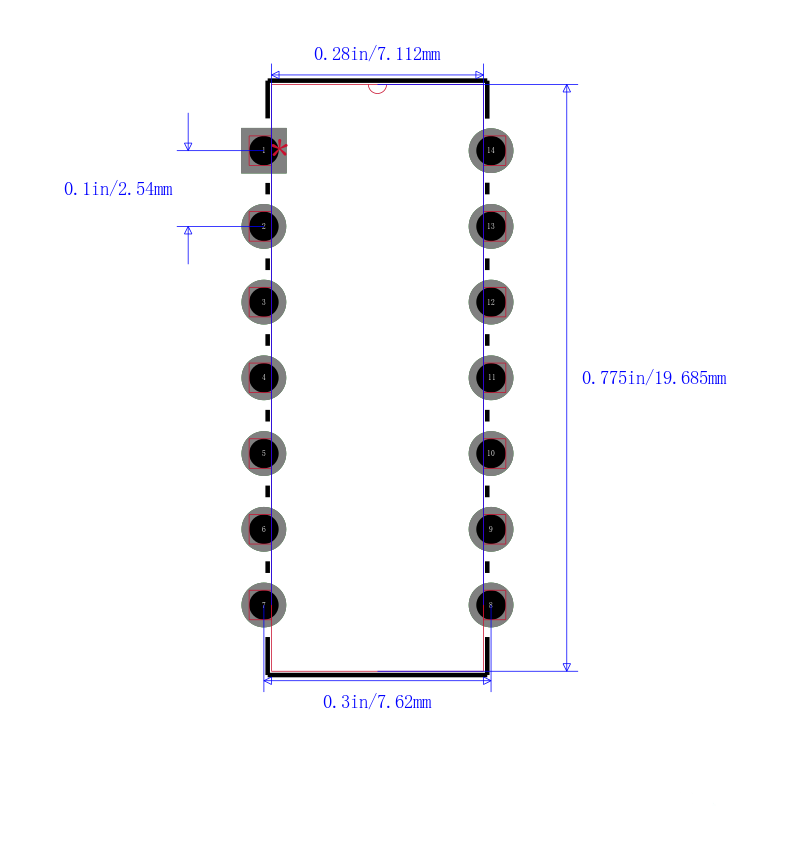
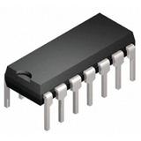
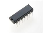
The PIC16F753/HV753 devices are covered by this data sheet. They are available in 14-pin PDIP, SOIC, TSSOP and 16-pin QFN packages. Block Diagrams and pinout descriptions of the devices are shown in Figure 1-1and Table 1- 1.
High-Performance RISC CPU:
• Only 35 Instructions to Learn:
- All single-cycle instructions except branches
• Operating Speed:
- DC – 20 MHz clock input
- DC – 200 ns instruction cycle
• 2048 x 14 On-chip Flash Program Memory
• Self Read/Write Program Memory
• 128 x 8 General Purpose Registers SRAM
• Interrupt Capability
• 8-Level Deep Hardware Stack
• Direct, Indirect and Relative Addressing modes
Microcontroller Features:
• Precision Internal Oscillator:
- Factory calibrated to ±1%, typical
- Software selectable frequency: 8 MHz, 4 MHz, 1 MHz or 31 kHz
- Software tunable
• Power-Saving Sleep mode
• Voltage Range PIC16F753:
- 2.0V to 5.5V
• Shunt Voltage Regulator PIC16HV753:
- 2.0V to user defined
- 5-volt regulation
- 1 mA to 50 mA shunt range
• Multiplexed Master Clear with Pull-up/Input Pin
• Interrupt-on-Change Pins
• Individually Programmable Weak Pull-ups
• Power-on Reset POR
• Power-up Timer PWRT
• Brown-out Reset BOR
• Watchdog Timer WDT with Internal Oscillator for Reliable Operation
• Industrial and Extended Temperature Range
• High Endurance Flash:
\- 100,000 write Flash endurance
\- Flash retention: >40 years
• Programmable Code Protection
• In-Circuit Debug ICD via Two Pins
• In-Circuit Serial Programming™ ICSP™ via Two Pins
Low-Power Features:
• Standby Current:
- 50 nA @ 2.0V, typical
• Operating Current:
- 11 uA @ 32 kHz, 2.0V, typical
- 260 uA @ 4 MHz, 2.0V, typical
• Watchdog Timer Current:
• <1 uA @ 2.0V, typical
Peripheral Features:
• 11 I/O Pins and one Input-only Pin
• High Current Source/Sink:
- 50 mA I/O, two pins
- 25 mA I/O, nine pins
• Two High-Speed Analog Comparator modules:
- 50 ns response time
- Fixed Voltage Reference FVR
- Programmable on-chip voltage reference via integrated 9-bit DAC
- Internal/external inputs and outputs selectable
- Built-in Hysteresis software selectable
• A/D Converter:
- 10-bit resolution
- Eight external channels
- Two internal reference voltage channels
• Operational Amplifier:
- Three terminal operations
- Internal connections to DAC and FVR
• Digital-to-Analog Converter DAC:
- 9-bit resolution
- Full Range output
- 4 mV steps @ 2.0V Limited Range
• Fixed Voltage Reference FVR, 1.2V Reference
• Capture, Compare, PWM CCP module:
- 16-bit Capture, max. resolution = 12.5 ns
- 16-bit Compare, max. resolution = 200 ns
- 10-bit PWM, max. frequency = 20 kHz
• Timer0: 8-Bit Timer/Counter with 8-Bit Prescaler
• Enhanced Timer1:
- 16-bit Timer/Counter with Prescaler
- External Timer1 Gate count enable
- Four Selectable Clock sources
• Timer2: 8-Bit Timer/Counter with Prescaler
- 8-Bit Period Register and Postscaler
• Two Hardware Limit Timers HLT:
- 8-bit Timer with Prescaler
- 8-bit period register and postscaler
- Asynchronous H/W Reset sources
• Complementary Output Generator COG:
- Complementary Waveforms from selectable sources
- Two I/O 50 mA for direct MOSFET drive
- Rising and/or Falling edge dead-band control
- Phase control, Blanking control
- Auto-shutdown
- Slope Compensation Circuit for use with SMPS power supplies