


40分之28引脚高性能,增强型闪存微控制器与CAN模块 28/40-Pin High-Performance, Enhanced Flash Microcontrollers with CAN Module
DEVICE OVERVIEW
This document contains device specific information for the following devices:
• PIC18F248
• PIC18F258
• PIC18F448
• PIC18F458
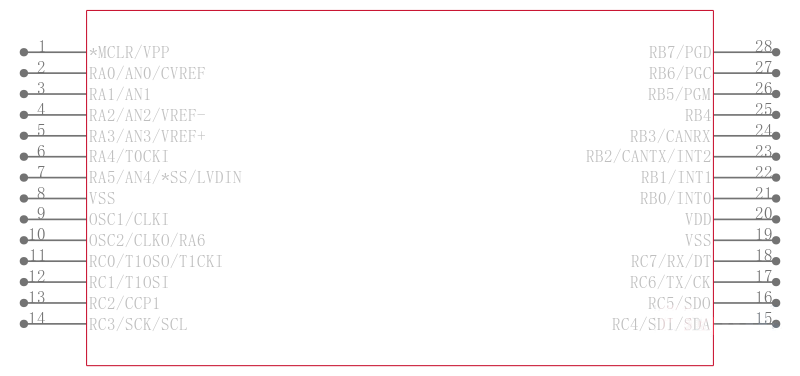
These devices are available in 28-pin, 40-pin and 44-pin packages. They are differentiated from each other in four ways:
1\. PIC18FX58 devices have twice the Flash program memory and data RAM of PIC18FX48 devices 32 Kbytes and 1536 bytes vs. 16 Kbytes and 768 bytes, respectively.
2\. PIC18F2X8 devices implement 5 A/D channels, as opposed to 8 for PIC18F4X8 devices.
3\. PIC18F2X8 devices implement 3 I/O ports, while PIC18F4X8 devices implement 5.
4\. Only PIC18F4X8 devices implement the Enhanced CCP module, analog comparators and the Parallel Slave Port.
All other features for devices in the PIC18FXX8 family, including the serial communications modules, are identical. These are summarized in Table 1-1. Block diagrams of the PIC18F2X8 and PIC18F4X8 devices are provided in Figure 1-1 and Figure 1-2, respectively. The pinouts for these device families are listed in Table 1-2.
High-Performance RISC CPU:
• Linear program memory addressing up to 2 Mbytes
• Linear data memory addressing to 4 Kbytes
• Up to 10 MIPS operation
• DC – 40 MHz clock input
• 4 MHz-10 MHz oscillator/clock input with PLL active
• 16-bit wide instructions, 8-bit wide data path
• Priority levels for interrupts
• 8 x 8 Single-Cycle Hardware Multiplier
Peripheral Features:
• High current sink/source 25 mA/25 mA
• Three external interrupt pins
• Timer0 module: 8-bit/16-bit timer/counter with 8-bit programmable prescaler
• Timer1 module: 16-bit timer/counter
• Timer2 module: 8-bit timer/counter with 8-bit period register time base for PWM
• Timer3 module: 16-bit timer/counter
• Secondary oscillator clock option – Timer1/Timer3
• Capture/Compare/PWM CCP modules; CCP pins can be configured as:
\- Capture input: 16-bit, max resolution 6.25 ns
\- Compare: 16-bit, max resolution 100 ns TCY
\- PWM output: PWM resolution is 1 to 10-bit
Max. PWM freq. @:8-bit resolution = 156 kHz
10-bit resolution = 39 kHz
• Enhanced CCP module which has all the features of the standard CCP module, but also has the following features for advanced motor control:
\- 1, 2 or 4 PWM outputs
\- Selectable PWM polarity
\- Programmable PWM dead time
• Master Synchronous Serial Port MSSP with two modes of operation:
\- 3-wire SPI™ Supports all 4 SPI modes
\- I2C™ Master and Slave mode
• Addressable USART module:
\- Supports interrupt-on-address bit
Advanced Analog Features:
• 10-bit, up to 8-channel Analog-to-Digital Converter module A/D with:
\- Conversion available during Sleep
\- Up to 8 channels available
• Analog Comparator module:
\- Programmable input and output multiplexing
• Comparator Voltage Reference module
• Programmable Low-Voltage Detection LVD module:
\- Supports interrupt-on-Low-Voltage Detection
• Programmable Brown-out Reset BOR CAN bus Module Features:
• Complies with ISO CAN Conformance Test
• Message bit rates up to 1 Mbps
• Conforms to CAN 2.0B Active Spec with:
\- 29-bit Identifier Fields
\- 8-byte message length
\- 3 Transmit Message Buffers with prioritization
\- 2 Receive Message Buffers
\- 6 full, 29-bit Acceptance Filters
\- Prioritization of Acceptance Filters
\- Multiple Receive Buffers for High Priority
Messages to prevent loss due to overflow
\- Advanced Error Management Features
Special Microcontroller Features:
• Power-on Reset POR, Power-up Timer PWRT and Oscillator Start-up Timer OST
• Watchdog Timer WDT with its own on-chip RC oscillator
• Programmable code protection
• Power-saving Sleep mode
• Selectable oscillator options, including:
\- 4x Phase Lock Loop PLL of primary oscillator
\- Secondary Oscillator 32 kHz clock input
• In-Circuit Serial ProgrammingTM ICSPTM via two pins
Flash Technology:
• Low-power, high-speed Enhanced Flash technology
• Fully static design
• Wide operating voltage range 2.0V to 5.5V
• Industrial and Extended temperature ranges
电源电压DC 5.00 V, 5.50 V max
时钟频率 40.0MHz max
RAM大小 768 x 8
耗散功率 1000 mW
I/O引脚数 23
存取时间 40.0 µs
内核架构 PIC
模数转换数ADC 1
工作温度Max 85 ℃
工作温度Min -40 ℃
耗散功率Max 1000 mW
电源电压Max 5.5 V
电源电压Min 2.5 V
安装方式 Surface Mount
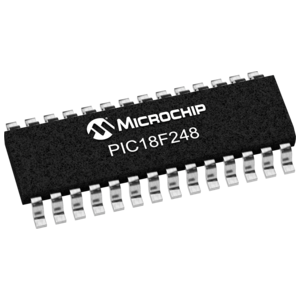
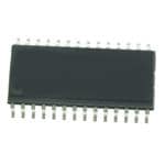
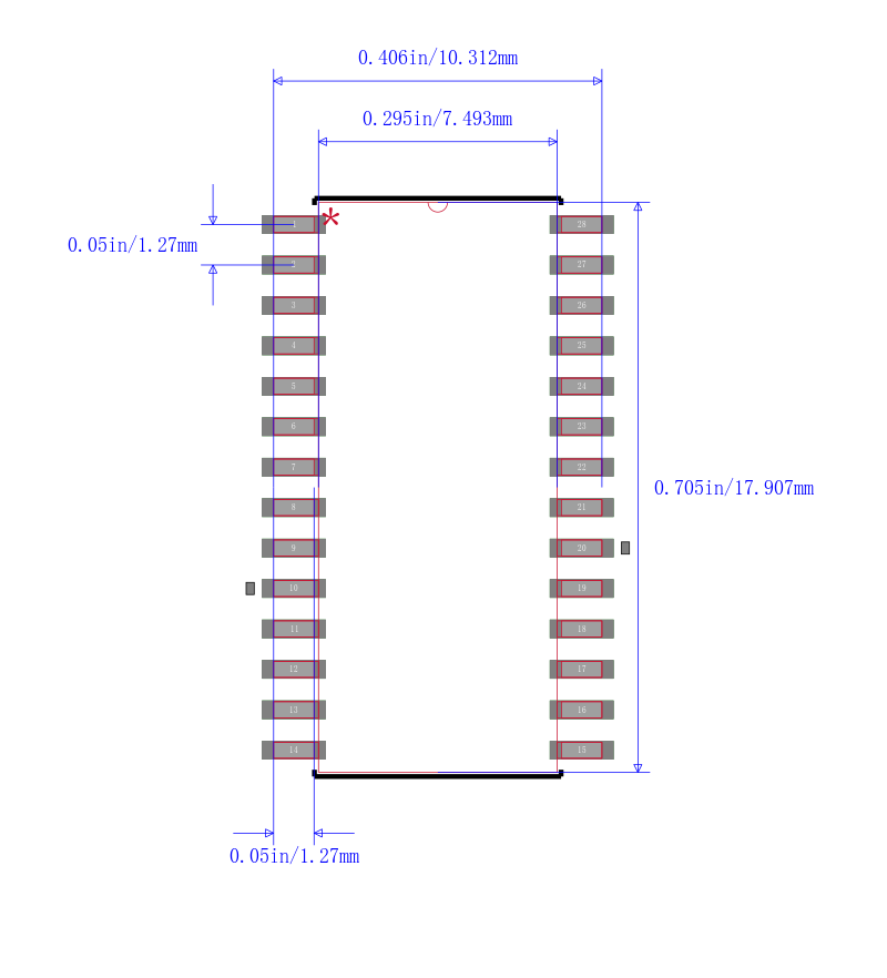
引脚数 28
封装 SOIC-28
长度 17.87 mm
宽度 7.49 mm
高度 2.31 mm
封装 SOIC-28
工作温度 -40℃ ~ 85℃
产品生命周期 Unknown
包装方式 Tube
RoHS标准 RoHS Compliant
含铅标准 Lead Free

| 型号/品牌 | 代替类型 | 替代型号对比 |
|---|---|---|
PIC18LF248-I/SO Microchip 微芯 | 当前型号 | 当前型号 |
PIC18LF248T-I/SO 微芯 | 完全替代 | PIC18LF248-I/SO和PIC18LF248T-I/SO的区别 |
PIC18LF2480-I/SO 微芯 | 类似代替 | PIC18LF248-I/SO和PIC18LF2480-I/SO的区别 |