输入/输出扩展, 8bit, 1 MHz, I2C, 2.3 V, 5.5 V, HVQFN
Overview
The PCA9670 provides general-purpose remote I/O expansion via the two-wire bidirectional I²C‑bus serial clock SCL, serial data SDA.
The devices consist of eight quasi-bidirectional ports, 1 MHz 30 mA drive I²C‑bus interface, three hardware address inputs and a reset input operating between 2.3 V and 5.5 V. 1 MHz I²C‑bus Fast‑mode Plus Fm+ can support PWM dimming of LEDs, and higher I²C‑bus drive 30 mA allows more devices to be on the bus without the need for bus buffers. The quasi-bidirectional port can be independently assigned as an input to monitor interrupt status or keypads, or as an output to activate indicator devices such as LEDs. The system master can read from the input port or write to the output port through a single register
The low current consumption of 2.5 μA typical, static is great for mobile applications and the latched output ports have 25 mA high current sink drive capability for directly driving LEDs.
The PCA9670 has three hardware address pins and allows up to 64 of these PCA9670 I/O expanders on the same I²C‑bus without the need for bus buffers, supporting up to 512 I/Os for example, 512 LEDs.
The internal Power-On Reset POR and active LOW hardware reset pin RESET initialize the I/Os as inputs with a weak internal pull-up 100 μA current source.
MoreLess
## Features
* I²C‑bus to parallel port expander
* 1 MHz I²C‑bus interface Fast-mode Plus I²C‑buss
* SDA with 30 mA sink capability for 4000 pF buses
* Operating supply voltage 2.3 V to 5.5 V with 5.5 V tolerant I/Os held to VDD with 100 μA current source
* 8-bit remote I/O pins that default to inputs at power-up
* Latched outputs with 25 mA sink capability for directly driving LEDs
* Total package sink capability of 200 mA
* Active LOW reset input
* Sixty-four programmable slave addresses using three address pins
* Readable device ID manufacturer, device type, and revision
* Software reset
* Low standby current 2.5 μA typical
* -40 °C to + 85 °C operation
* ESD protection exceeds 2000 V HBM per JESD22-A114 and 1000 V CDM per JESD22‑C101
* Latch-up testing is done to JEDEC standard JESD78 which exceeds 100 mA
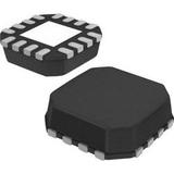
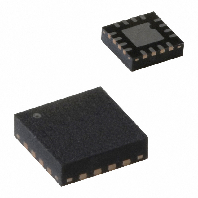
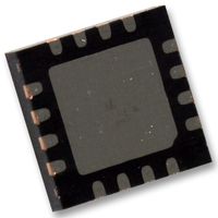
* Packages offered: SO16, TSSOP16, HVQFN16
## Target Applications
* LED signs and displays
* Servers
* Keypads
* Industrial control
* Medical equipment
* PLCs
* Cellular telephones
* Mobile devices
* Gaming machines
* Instrumentation and test measurement
## Features