电平转换I2C总线中继器, 2输入, 0.9 V至5.5 V电源, TSSOP-8
Overview
The PCA9508 is a CMOS integrated circuit that supports hot-swap with zero offset and provides level shifting between low voltage down to 0.9 V and higher voltage 2.7 V to 5.5 V for I²C-bus or SMBus applications. While retaining all the operating modes and features of the I²C-bus system during the level shifts, it also permits extension of the I²C-bus by providing bidirectional buffering for both the data SDA and the clock SCL lines, thus enabling two buses of 400 pF. Using the PCA9508 enables the system designer to isolate two halves of a bus for both voltage and capacitance, and perform hot-swap and voltage level translation. Furthermore, the dual supply pins can be powered up in any sequence; when any of the supply pins are unpowered, the 5 V tolerant I/O are high-impedance.
The hot swap feature allows an I/O card to be inserted into a live backplane without corrupting the data and clock buses. Control circuitry prevents the backplane from being connected to the card until a stop command or bus idle occurs on the backplane without bus contention on the card. Zero offset output voltage allows multiple PCA9508s to be put in series and still maintains an excellent noise margin.
PCA9508 has B side and A side bus drivers. The 2.7 V to 5.5 V bus B side drivers behave much like the drivers on the PCA9515A device, while the adjustable voltage bus A side drivers drive more current and incur no static offset voltage. This results in a LOW on the B side translating into a nearly 0 V LOW on the A side.
The static offset design of the B side PCA9508 I/O drivers prevents them from being connected to another device that has a rise time accelerator including the PCA9510/A, PCA9511/A, PCA9512/A, PCA9513/A, or PCA9514/A or a static offset voltage including the PCA9507 B side, PCA9508 B side, PCA9509 A side, PCA9515/A, PCA9516A, PCA9517/A B side, PCA9518, PCA9519 A side, or P82B96/PCA9600 Sx/Sy side. The A side of two or more PCA9508s can be connected together, however, to allow a star topology with the A side on the common bus, and the A side can be connected directly to any other buffer with static or dynamic offset voltage. Multiple PCA9508s can be connected in series, A side to B side, with no build-up in offset voltage with only time-of-flight delays to consider.
The PCA9508 drivers are not enabled unless the bus is idle, VCCA is above 0.8 V and VCCB is above 2.5 V. The EN pin can also be used to turn the drivers on and off under system control. Caution should be observed to only change the state of the enable pin when the bus is idle.
The output pull-down on the B side internal buffer LOW is set for approximately 0.5 V, while the input threshold of the internal buffer is set about 70 mV lower 0.43 V. When the B side I/O is driven LOW internally, the LOW is not recognized as a LOW by the input. This prevents a lock-up condition from occurring. The output pull-down on the A side drives a hard LOW and the input level is set at 0.5VCCA to accommodate the need for a lower LOW level in systems where the low voltage side supply voltage is as low as 0.9 V.
MoreLess
## Features
* 2 channel, bidirectional buffer isolates capacitance and allows 400 pF on either side of the device
* Supports offset-free hot-swap with IDLE/STOP detect circuitry
* Voltage level translation from 0.9 V to 5.5 V and from 2.7 V to 5.5 V
* Footprint and functional replacement for PCA9515, PCA9515A, PCA9517 and PCA9517A
* I²C-bus and SMBus compatible
* Active HIGH repeater enable input
* Static level offset on B side
* Open-drain input/outputs
* Lock-up free operation
* Supports arbitration and clock stretching across the repeater
* Accommodates Standard-mode and Fast-mode I²C-bus devices and multiple masters
* Powered-off high-impedance I²C-bus pins
* A side operating supply voltage range of 0.9 V to 5.5 V
* B side operating supply voltage range of 2.7 V to 5.5 V
* 5 V tolerant I²C-bus and enable pins
* 0 Hz to 400 kHz clock frequency the maximum system operating frequency may be less than 400 kHz because of the delays added by the repeater.
* ESD protection exceeds 6000 V HBM per JESD22-A114, 450 V MM per JESD22-A115, and 1000 V CDM per JESD22-C101
* Latch-up testing is done to JEDEC Standard JESD78 which exceeds 100 mA
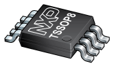
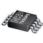
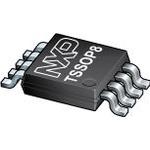
* Packages offered: SO8 and TSSOP8
## Features
供电电流 1 mA
通道数 1
针脚数 8
耗散功率 100 mW
输入电容 5.2 pF
输入数 2
工作温度Max 85 ℃
工作温度Min -40 ℃
耗散功率Max 100 mW
电源电压 2.7V ~ 5.5V
电源电压Max 5.5 V
安装方式 Surface Mount
引脚数 8
封装 TSSOP-8
封装 TSSOP-8
工作温度 -40℃ ~ 85℃
产品生命周期 Active
包装方式 Tape & Reel TR
制造应用 I²C - 热插拔
RoHS标准 RoHS Compliant
含铅标准 Lead Free
ECCN代码 EAR99