


专用接口, I2C, SMBus, I2C总线与SMBus系统应用, 3 V, 5.5 V, TSSOP, 20 引脚
Overview
The PCA9519 is a 4-channel level translating I²C-bus/SMBus repeater that enables the processor low voltage 2-wire serial bus to interface with standard I²C-bus or SMBus I/O. While retaining all the operating modes and features of the I²C-bus system during the level shifts, it also permits extension of the I²C-bus by providing bidirectional buffering for both the data SDA and the clock SCL lines, thus enabling the I²C-bus or SMBus maximum capacitance of 400 pF on the higher voltage side. The SDA and SCL pins are over-voltage tolerant and are high-impedance when the PCA9519 is unpowered.
The port B drivers are compliant with SMBus I/O levels, while port A uses a current sensing mechanism to detect the input or output LOW signal which prevents bus lock-up. The port A uses a 1 mA current source for pull-up and a 200 Ω pull-down driver. This results in a LOW on port A accommodating smaller voltage swings. The output pull-down on the port A internal buffer LOW is set for approximately 0.2 V, while the input threshold of the internal buffer is set about 50 mV lower than that of the output voltage LOW. When the port A I/O is driven LOW internally, the LOW is not recognized as a LOW by the input. This prevents a lock-up condition from occurring. The output pull-down on the port B drives a hard LOW and the input level is set at 0.3 of SMBus or I²C-bus voltage level which enables port B to connect to any other I²C-bus device or buffer.
The PCA9519 drivers are not enabled unless VCCA is above 0.8 V and VCCB is above 2.5 V. The enable EN pin can also be used to turn the drivers on and off under system control. Caution should be observed to only change the state of the EN pin when the bus is idle.
MoreLess
## Features
* 4-channel 4 SCL/SDA pairs, bidirectional buffer isolates capacitance and allows 400 pF on port B of the device
* Voltage level translation from port A 1 V to VCCB \\- 1.5 V to port B 3.0 V to 5.5 V
* Requires no external pull-up resistors on lower voltage port A
* Active HIGH repeater enable input
* Open-drain inputs/outputs
* Lock-up free operation
* Supports arbitration and clock stretching across the repeater
* Accommodates Standard-mode and Fast-mode I²C-bus devices and multiple masters
* Powered-off high-impedance I²C-bus pins
* Operating supply voltage range of 1.0 V to VCCB \\- 1.5 V on port A, 3.0 V to 5.5 V on port B
* 5 V tolerant B-side SCL and SDA and enable pins
* 50 ns glitch filter on B-side input
* 0 Hz to 400 kHz clock frequency
**Remark:** The maximum system operating frequency may be less than 400 kHz because of the delays added by the repeater.
* ESD protection exceeds 2000 V HBM per JESD22-A114 and 1000 V CDM per JESD22-C101
* Latch-up testing is done to JEDEC Standard JESD78 which exceeds 100 mA
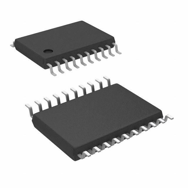
* Packages offered: TSSOP20, HVQFN24
## Features
供电电流 11.6 mA
通道数 4
针脚数 20
耗散功率 100 mW
输入电容 6 pF
工作温度Max 85 ℃
工作温度Min -40 ℃
耗散功率Max 100 mW
电源电压 3V ~ 5.5V
电源电压Max 5.5 V
电源电压Min 1 V
安装方式 Surface Mount
引脚数 20
封装 TSSOP-20
封装 TSSOP-20
工作温度 -40℃ ~ 85℃
产品生命周期 Active
包装方式 Tape & Reel TR
制造应用 I²C
RoHS标准 RoHS Compliant
含铅标准 Lead Free
ECCN代码 EAR99
| 型号/品牌 | 代替类型 | 替代型号对比 |
|---|---|---|
PCA9519PW,118 NXP 恩智浦 | 当前型号 | 当前型号 |
PCA9519PW,112 恩智浦 | 功能相似 | PCA9519PW,118和PCA9519PW,112的区别 |