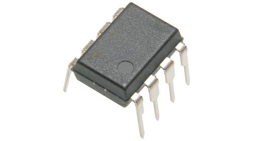
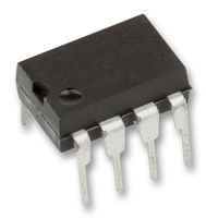
NXP PCF8583P 芯片, 时钟/日历/SRAM
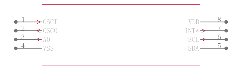
The is a Clock and Calendar Chip, based on a 2048 bit static CMOS RAM organized as 256 words by 8 bits. Addresses and data are transferred serially via the two-line bidirectional I²C-bus. The built-in word address register is incremented automatically after each written or read data byte. Address pin A0 is used for programming the hardware address, allowing the connection of two devices to the bus without additional hardware. The built-in 32.768kHz oscillator circuit and the first 8bytes of the RAM are used for the clock, calendar and counter functions. The next 8bytes can be programmed as alarm registers or used as free RAM space. The remaining 240bytes are free RAM locations.
- .
- 50µA Maximum Operating current at fSCL = 0Hz
- .
- Clock function with four year calendar
- .
- Universal timer with alarm and overflow indication
- .
- 24- or 12-hour format
- .
- 32.768kHz or 50Hz time base
- .
- Serial input and output bus I²C-bus
- .
- Automatic word address incrementing
ESD sensitive device, take proper precaution while handling the device.
| 型号/品牌 | 代替类型 | 替代型号对比 |
|---|---|---|
PCF8583P NXP 恩智浦 | 当前型号 | 当前型号 |
PCF8583P/F5,112 恩智浦 | 完全替代 | PCF8583P和PCF8583P/F5,112的区别 |
PCF8583PN 恩智浦 | 完全替代 | PCF8583P和PCF8583PN的区别 |