


I2C总线远程8位I/O扩展器
Overview
The PCF8574/74A provides general-purpose remote I/O expansion via the two-wire bidirectional I²C‑bus serial clock SCL, serial data SDA.
The devices consist of eight quasi-bidirectional ports, 100 kHz I²C‑bus interface, three hardware address inputs and interrupt output operating between 2.5 V and 6 V. The quasi-bidirectional port can be independently assigned as an input to monitor interrupt status or keypads, or as an output to activate indicator devices such as LEDs. System master can read from the input port or write to the output port through a single register.
The low current consumption of 2.5 μA typical, static is great for mobile applications and the latched output ports directly drive LEDs.
The PCF8574 and PCF8574A are identical, except for the different fixed portion of the slave address. The three hardware address pins allow eight of each device to be on the same I²C‑bus, so there can be up to 16 of these I/O expanders PCF8574/74A together on the same I²C‑bus, supporting up to 128 I/Os for example, 128 LEDs.
The active LOW open-drain interrupt output INT can be connected to the interrupt logic of the microcontroller and is activated when any input state differs from its corresponding input port register state. It is used to indicate to the microcontroller that an input state has changed and the device needs to be interrogated without the microcontroller continuously polling the input register via the I²C‑bus.
The internal Power-On Reset POR initializes the I/Os as inputs with a weak internal pull-up 100 μA current source.
MoreLess
## Features
* I²C-bus to parallel port expander
* 100 kHz I²C‑bus interface Standard-mode I²C-bus
* Operating supply voltage 2.5 V to 6 V with non-overvoltage tolerant I/O held to VDD with 100 μA current source
* 8-bit remote I/O pins that default to inputs at power-up
* Latched outputs directly drive LEDs
* Total package sink capability of 80 mA
* Active LOW open-drain interrupt output
* Eight programmable slave addresses using three address pins
* Low standby current 2.5 μA typical
* -40 °C to +85 °C operation
* ESD protection exceeds 2000 V HBM per JESD22-A114 and 1000 V CDM per JESD22-C101
* Latch-up testing is done to JEDEC standard JESD78 which exceeds 100 mA
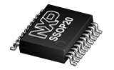
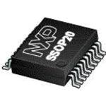
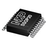
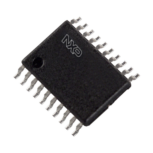
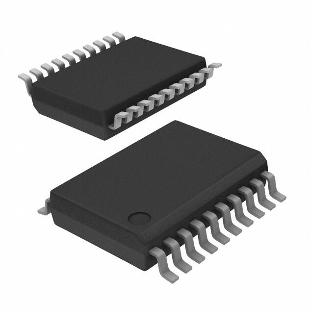
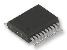
* Packages offered: DIP16, SO16, SSOP20
## Target Applications
* LED signs and displays
* Servers
* Key pads
* Industrial control
* Medical equipment
* PLC
* Cellular telephones
* Mobile devices
* Gaming machines
* Instrumentation and test measurement
## Features
电源电压DC 2.50V min
输出电流 25 mA
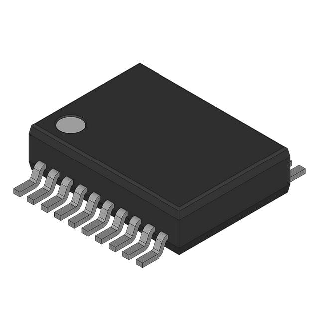
针脚数 20
时钟频率 100 kHz
耗散功率 400 mW
输入/输出数 8 Input
工作温度Max 85 ℃
工作温度Min -40 ℃
电源电压 2.5V ~ 6V
电源电压Max 6 V
电源电压Min 2.5 V
安装方式 Surface Mount
引脚数 20
封装 SSOP-20
封装 SSOP-20
工作温度 -40℃ ~ 85℃
产品生命周期 Active
包装方式 Tape & Reel TR
RoHS标准 RoHS Compliant
含铅标准 Lead Free
ECCN代码 EAR99
| 型号/品牌 | 代替类型 | 替代型号对比 |
|---|---|---|
PCF8574TS/3,118 NXP 恩智浦 | 当前型号 | 当前型号 |
PCF8574ATS/3,118 恩智浦 | 完全替代 | PCF8574TS/3,118和PCF8574ATS/3,118的区别 |
PCF8574TS/3,112 恩智浦 | 完全替代 | PCF8574TS/3,118和PCF8574TS/3,112的区别 |
PCF8574TS/3 恩智浦 | 完全替代 | PCF8574TS/3,118和PCF8574TS/3的区别 |