
时钟和日历, 240 ×8位的RAM Clock and calendar with 240 x 8-bit RAM
General description
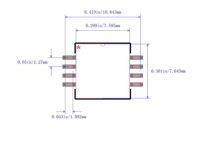
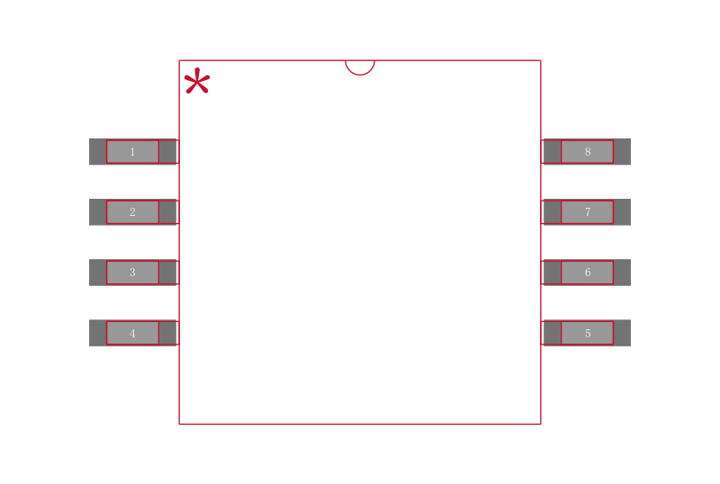
The PCF8583 is a clock and calendar chip, based on a 2048 bit static CMOS1 RAM organized as 256 words by 8 bits. Addresses and data are transferred serially via the two-line bidirectional I2C-bus. The built-in word address register is incremented automatically after each written or read data byte. Address pin A0 is used for programming the hardware address, allowing the connection of two devices to the bus without additional hardware.
The built-in 32.768 kHz oscillator circuit and the first 8 bytes of the RAM are used for the clock, calendar, and counter functions. The next 8 bytes can be programmed as alarm registers or used as free RAM space. The remaining 240 bytes are free RAM locations.
Features and benefits
I2C-bus interface operating supply voltage: 2.5 V to 6 V
Clock operating supply voltage 1.0 V to 6.0 V at 0°Cto+70°C
240×8-bit low-voltage RAM
Data retention voltage: 1.0 V to 6.0 V
Operating current at fSCL= 0 Hz: max 50 μA
Clock function with four year calendar
Universal timer with alarm and overflow indication
24 hour or 12 hour format
32.768 kHz or 50 Hz time base
Serial input and output bus I2C-bus
Automatic word address incrementing
Programmable alarm, timer, and interrupt function
Slave addresses: A1h or A3h for reading, A0h or A2h for writing