
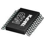
NXP PCA9848PWJ 芯片, 开关, 双路, 8:1, TSSOP-24 新
Overview
The PCA9848 is an ultra-low voltage, octal bidirectional translating switch controlled via the I²C-bus. The SCL/SDA upstream pair fans out to eight downstream pairs, or channels. Any or all SCx/SDx channels can be selected, determined by the programmable control register. This feature allows multiple devices with the same I²C-bus address to reside on the same bus. The switch device can also separate a heavily loaded I²C-bus into separate bus segments, eliminating the need for a bus buffer.
An active LOW reset input allows the PCA9848 to recover from a situation where one of the downstream I²C-buses is stuck in a LOW state. Pulling the RESET pin LOW resets the I²C-bus state machine and deselects all the channels, as does the internal Power-On Reset POR function.
The pass gates of the switches are constructed such that the VDD1 pin is used to limit the maximum high voltage which is passed by the PCA9848. This allows the use of different bus voltages on each channel, so that 0.8 V, 1.8 V, 2.5 V or 3.3 V parts can communicate without any additional protection. External pull-up resistors pull the bus up to the desired voltage level for each channel. All I/O pins are 3.6 V tolerant.
MoreLess
## Features
* Ultra-low voltage operation, down to 0.8 V to interface with next-generation CPUs
* 1-of-8 bidirectional translating switch
* Fm+ I²C-bus interface logic; compatible with SMBus standards
* Active LOW reset input
* 2 address pins allowing up to 16 devices on the I²C-bus
* Channel selection via I²C-bus
* Power-up with all switch channels deselected
* Low Ron switches
* Allows voltage level translation between 0.8 V, 1.8 V, 2.5 V and 3.3 V buses
* Reset via I²C-bus software command
* I²C Device ID function
* No glitch on power-up
* Supports hot insertion since all channels are de-selected at power-on
* Low standby current
* 3.6 V tolerant inputs
* 0 Hz to 1 MHz clock frequency
* ESD protection exceeds 6000 V HBM per JESD22-A114 and 1000 V CDM per JESD22-C101
* Latch-up testing is done to JEDEC Standard JESD78 which exceeds 100 mA
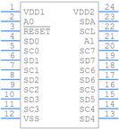
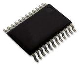
* Two packages offered: TSSOP24 and HVQFN24
## Features