时钟倍频器, 抖动衰减器, 1.4GHz, 1.71V至1.89V, 2输出, QFN-36
Description
The Si5326 is a jitter-attenuating precision clock multiplier for applications requiring sub 1 ps jitter performance. The Si5326 accepts two input clocks ranging from 2 kHz to 710 MHz and generates two output clocks ranging from 2 kHz to 945 MHz and select frequencies to 1.4 GHz. The two outputs are divided down separately from a common source. The Si5326 can also use its crystal oscillator as a clock source for frequency synthesis. The device provides virtually any frequency translation combination across this operating range. The Si5326 input clock frequency and clock multiplication ratio are programmable through an I2C or SPI interface.
Features
Generates any frequency from 2 kHz to 945 MHz and select frequencies to 1.4 GHz from an input frequency of 2 kHz to 710 MHz
Ultra-low jitter clock outputs with jitter generation as low as 0.3 ps rms50 kHz–80 MHz
Integrated loop filter with selectable loop bandwidth 60 Hz to 8.4 kHz
Meets OC-192 GR-253-CORE jitter specifications
Dual clock inputs with manual or automatically controlled hitless switching LVPECL, LVDS, CML, CMOS
Dual clock outputs with selectable signal format
Support for ITU G.709 and custom FEC ratios 255/238, 255/237, 255/236
LOL, LOS, FOS alarm outputs
Digitally-controlled output phase adjustment
I2C or SPI programmable
On-chip voltage regulator for 1.8 ±5%, 2.5 ±10%, or 3.3 V ±10% operation
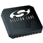
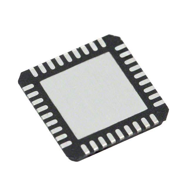
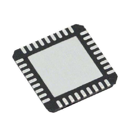
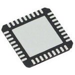
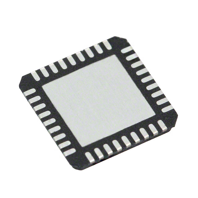
Small size: 6 x 6 mm 36-lead QFN
Pb-free, ROHS compliant
Applications
SONET/SDH OC-48/OC-192/STM-16/STM-64 line cards
ITU G.709 and custom FEC line cards
GbE/10GbE, 1/2/4/8/10G Fibre Channel line cards
GbE/10GbE Synchronous Ethernet
Optical modules
Wireless basestations
Data converter clocking
xDSL
PDH clock synthesis
Test and measurement
Broadcast video
| 型号/品牌 | 代替类型 | 替代型号对比 |
|---|---|---|
SI5326A-C-GM Silicon Labs 芯科 | 当前型号 | 当前型号 |
SI5326B-C-GMR 芯科 | 完全替代 | SI5326A-C-GM和SI5326B-C-GMR的区别 |
SI5326A-C-GMR 芯科 | 完全替代 | SI5326A-C-GM和SI5326A-C-GMR的区别 |
SI5326C-C-GMR 芯科 | 完全替代 | SI5326A-C-GM和SI5326C-C-GMR的区别 |