

数字信号处理器 Digital Signal Processors
Introduction
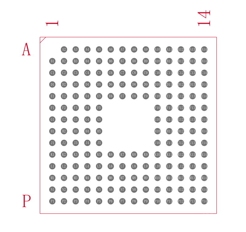
This section provides a summary of each device’s features, lists the pin assignments, and describes the
function of each pin. This document also provides detailed descriptions of peripherals, electrical
specifications, parameter measurement information, and mechanical data about the available packaging.
Description
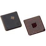
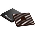
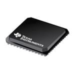
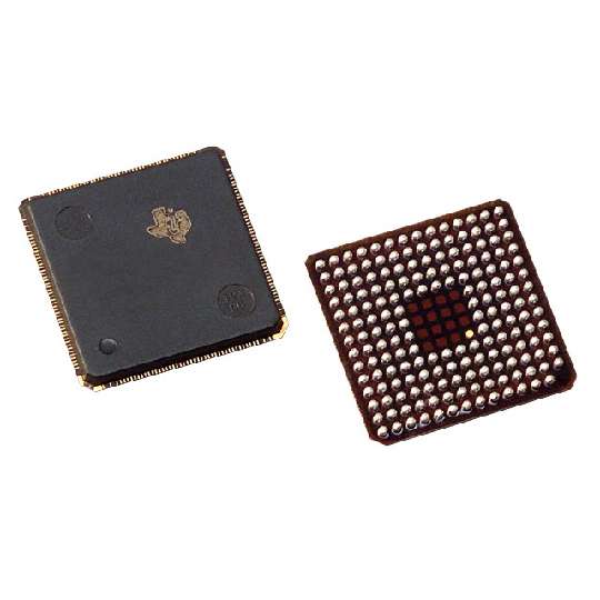
The SM320F2810-EP, SM320F2811-EP, SM320F2812-EP, SM320C2810-EP, SM320C2811-EP, and M320C2812-EP devices, members of the TMS320C28xDSP generation, are highly integrated, high-performance solutions for demanding control applications. The functional blocks and the memory maps are described in Section 3, Functional Overview.
Features
Controlled Baseline
− One Assembly/Test/Fabrication Site
Extended Temperature Performance of
−55°C to 125°C
Enhanced Diminishing Manufacturing Sources DMS Support
Enhanced Product-Change Notification
Qualification Pedigree†
High-Performance Static CMOS Technology
− 150 MHz 6.67-ns Cycle Time
− Low-Power 1.8-V Core @135 MHz, 1.9-V Core @150 MHz, 3.3-V I/O Design JTAG Boundary Scan Support‡
High-Performance 32-Bit CPU 320C28x
− 16 x 16 and 32 x 32 MAC Operations
− 16 x 16 Dual MAC
− Harvard Bus Architecture
− Atomic Operations
− Fast Interrupt Response and Processing
− Unified Memory Programming Model
− 4M Linear Program/Data Address Reach
− Code-Efficient in C/C++ and Assembly
− 320F24x/LF240x Processor Source Code Compatible
On-Chip Memory
− Flash Devices: Up to 128K x 16 Flash Four 8K x 16 and Six 16K x 16 Sectors
− ROM Devices: Up to 128K x 16 ROM
− 1K x 16 OTP ROM
− L0 and L1: 2 Blocks of 4K x 16 Each Single-Access RAM SARAM
− H0: 1 Block of 8K x 16 SARAM
− M0 and M1: 2 Blocks of 1K x 16 Each SARAM
Boot ROM 4K x 16
− With Software Boot Modes
− Standard Math Tables
External Interface 2812
− Up to 1M Total Memory
− Programmable Wait States
− Programmable Read/Write Strobe Timing
− Three Individual Chip Selects
| 型号/品牌 | 代替类型 | 替代型号对比 |
|---|---|---|
SM320F2812GHHMEP TI 德州仪器 | 当前型号 | 当前型号 |
TMS320F2812ZHHA 德州仪器 | 类似代替 | SM320F2812GHHMEP和TMS320F2812ZHHA的区别 |
TMS320F2812GHHA 德州仪器 | 类似代替 | SM320F2812GHHMEP和TMS320F2812GHHA的区别 |
TMS320F2812ZHHS 德州仪器 | 类似代替 | SM320F2812GHHMEP和TMS320F2812ZHHS的区别 |