


具有预加重和 IEEE 1149.6 功能的 1.5Gbps 2x2 LVDS 交叉点开关 32-LQFP -40 to 85
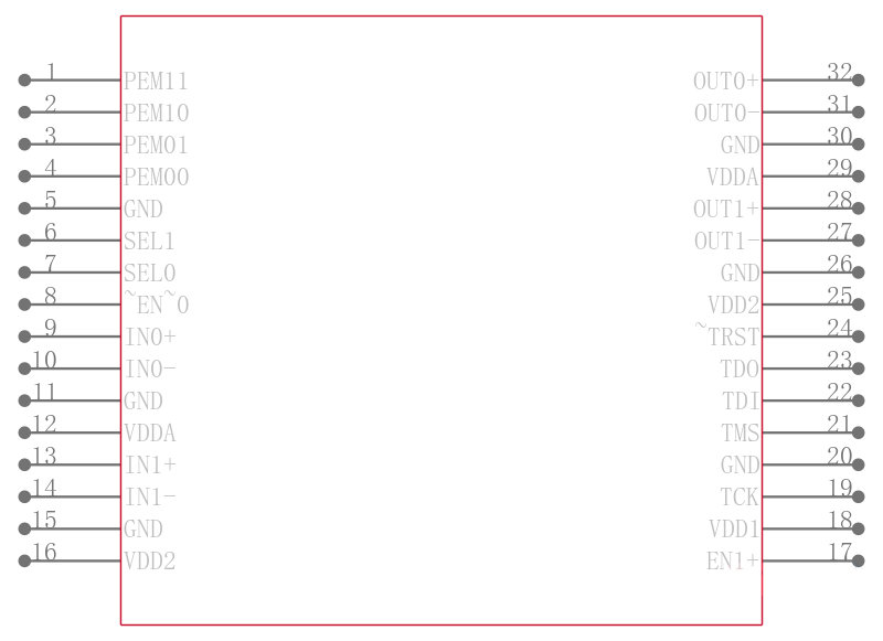
The SCAN90CP02 is a 1.5 Gbps 2 x 2 LVDS crosspoint switch. High speed data paths and flow-through pinout minimize internal device jitter, while configurable 0/25/50/100% pre-emphasis overcomes external ISI jitter effects of lossy backplanes and cables. The differential inputs interface to LVDS and Bus LVDS signals such as those on "s 10-, 16-, and 18- bit Bus LVDS SerDes, as well as CML and LVPECL. The SCAN90CP02 can also be used with ASICs and FPGAs. The non-blocking crosspoint architecture is pin-configurable as a 1:2 clock or data splitter, 2:1 redundancy mux, crossover function, or dual buffer for signal booster and stub hider applications.
Integrated IEEE 1149.1 JTAG and 1149.6 circuitry supports testability of both single-ended LVTTL/CMOS and differential LVDS PCB interconnect. The 3.3V supply, CMOS process, and LVDS I/O ensure high performance at low power over the entire industrial -40 to +85°C temperature range.
| 型号/品牌 | 代替类型 | 替代型号对比 |
|---|---|---|
SCAN90CP02VY/NOPB TI 德州仪器 | 当前型号 | 当前型号 |
SCAN90CP02VYX/NOPB 德州仪器 | 完全替代 | SCAN90CP02VY/NOPB和SCAN90CP02VYX/NOPB的区别 |
SCAN90CP02VY 美国国家半导体 | 功能相似 | SCAN90CP02VY/NOPB和SCAN90CP02VY的区别 |
SCAN90CP02VYX 德州仪器 | 功能相似 | SCAN90CP02VY/NOPB和SCAN90CP02VYX的区别 |