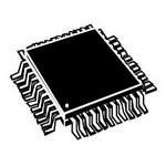
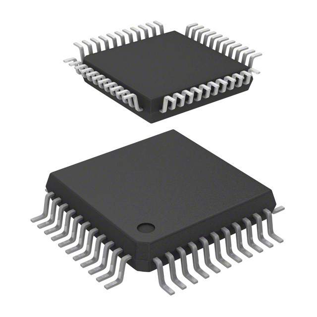


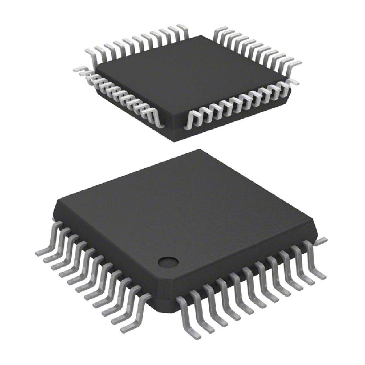
有8到32K闪存, 10位ADC , 4个定时器, SPI , SCI接口5V范围8位MCU 5V RANGE 8-BIT MCU WITH 8 TO 32K FLASH,10-BIT ADC, 4 TIMERS,SPI,SCI INTERFACE
INTRODUCTION
The ST72324 devices are members of the ST7 microcontroller family designed for the 5V operating range.
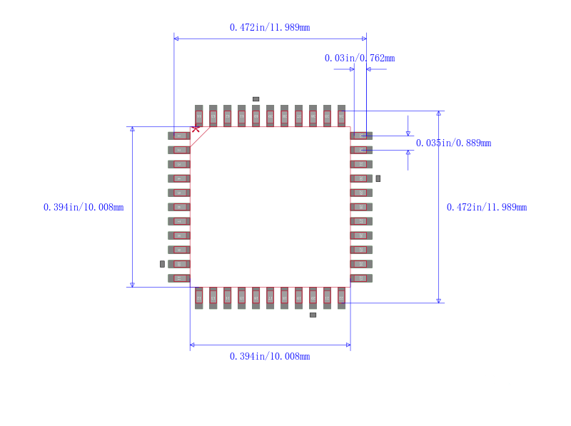
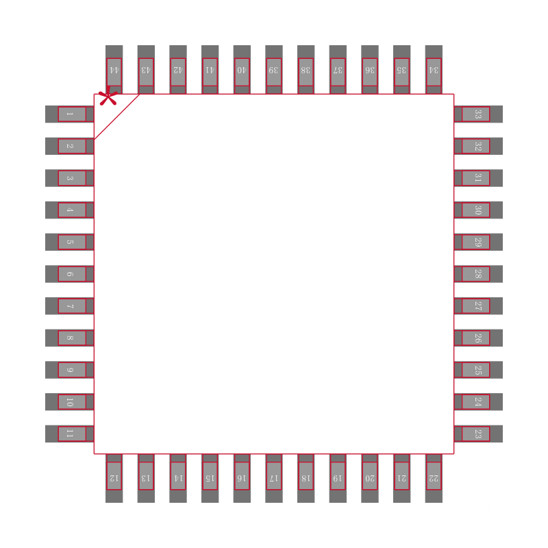
– The 32-pin devices are designed for mid-range applications
– The 42/44-pin devices target the same range of applications requiring more than 24 I/O ports.
For a description of the differences between ST72324 and ST72324B devices refer to Section 14.2 on page 152
All devices are based on a common industry standard 8-bit core, featuring an enhanced instruction set and are available with FLASH program memory.
Under software control, all devices can be placed in WAIT, SLOW, ACTIVE-HALT or HALT mode, reducing power consumption when the application is in idle or stand-by state.
The enhanced instruction set and addressing modes of the ST7 offer both power and flexibility to software developers, enabling the design of highly efficient and compact application code. In addition to standard 8-bit data management, all ST7 microcontrollers feature true bit manipulation, 8x8 unsigned multiplication and indirect addressing modes.
■ Memories
– 8 to 32K dual voltage High Density Flash HD Flash with read-out protection capability. In Application Programming and In-Circuit Programming for HDFlash devices
– 384 to 1K bytes RAM
– HDFlash endurance: 100 cycles, data retention: 20 years at 55°C
■ Clock, Reset And Supply Management
– Enhanced low voltage supervisor LVD for main supply with programmable reset thresh olds and auxiliary voltage detector AVD with interrupt capability
– Clock sources: crystal/ceramic resonator oscillators, internal RC oscillator, clock security system and bypass for external clock
– PLL for 2x frequency multiplication
– Four Power Saving Modes: Halt, Active-Halt, Wait and Slow
■ Interrupt Management
– Nested interrupt controller
– 10 interrupt vectors plus TRAP and RESET
– 9/6 external interrupt lines on 4 vectors
■ Up to 32 I/O Ports
– 32/24 multifunctional bidirectional I/O lines
– 22/17 alternate function lines
– 12/10 high sink outputs
■ 4 Timers
– Main Clock Controller with: Real time base, Beep and Clock-out capabilities
– Configurable watchdog timer
– 16-bit Timer A with: 1 input capture, 1 output compare, external clock input, PWM and pulse generator modes
– 16-bit Timer B with: 2 input captures, 2 output compares, PWM and pulse generator modes
■ 2 Communication Interfaces
– SPI synchronous serial interface
– SCI asynchronous serial interface
■ 1 Analog Peripheral low current coupling
– 10-bit ADC with up to 12 robust input ports
■ Instruction Set
– 8-bit Data Manipulation
– 63 Basic Instructions
– 17 main Addressing Modes
– 8 x 8 Unsigned Multiply Instruction
■ Development Tools
– Full hardware/software development package
– In-Circuit Testing capability

| 型号/品牌 | 代替类型 | 替代型号对比 |
|---|---|---|
ST72F324J6T5 ST Microelectronics 意法半导体 | 当前型号 | 当前型号 |
ST72F324J6T6 意法半导体 | 类似代替 | ST72F324J6T5和ST72F324J6T6的区别 |
ST72F324J6TA 意法半导体 | 类似代替 | ST72F324J6T5和ST72F324J6TA的区别 |
ST72F324J6TC 意法半导体 | 类似代替 | ST72F324J6T5和ST72F324J6TC的区别 |