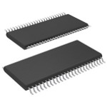
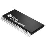
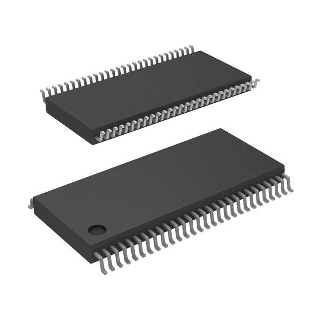

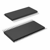


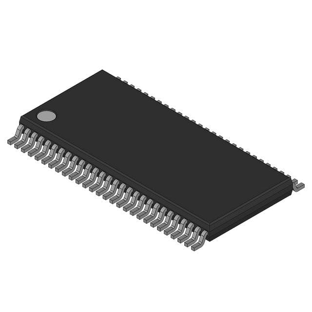
具有三态输出的 16 位总线收发器和寄存器 56-TSSOP -40 to 85
This 16-bit bus transceiver and register is designed for 1.65-V to 3.6-V VCC operation.
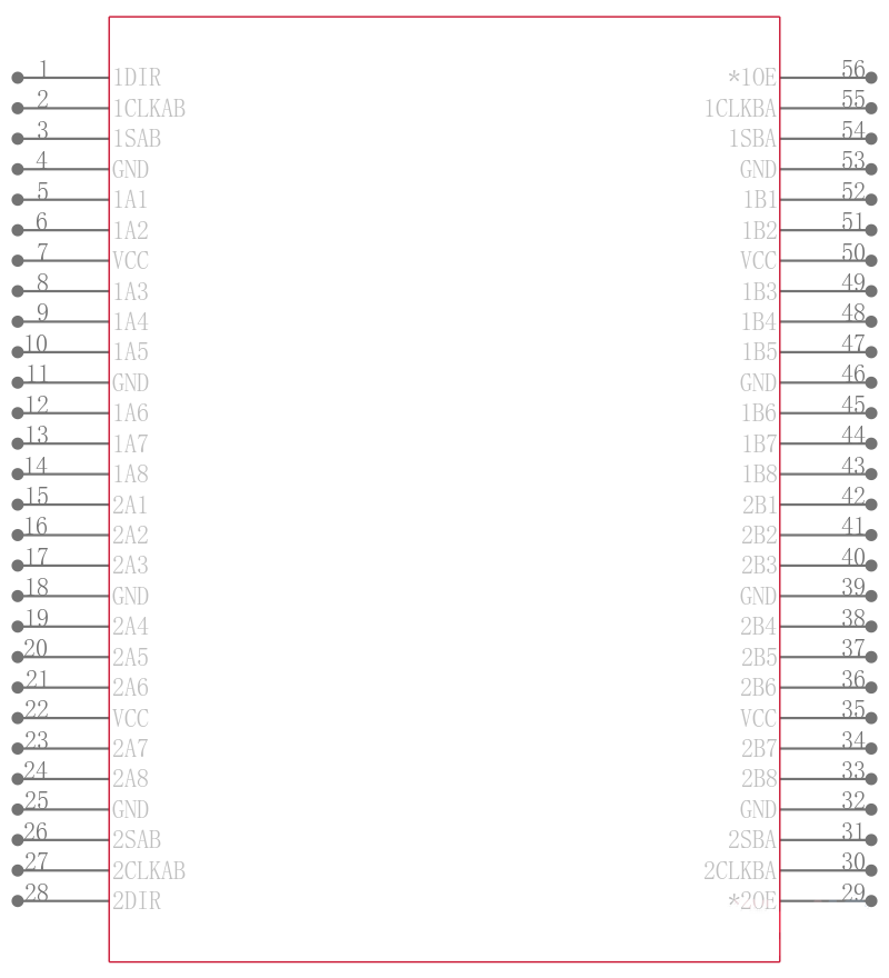
The SN74ALVCH16646 can be used as two 8-bit transceivers or one 16-bit transceiver. Data on the A or B bus is clocked into the registers on the low-to-high transition of the appropriate clock CLKAB or CLKBA input. Figure 1 illustrates the four fundamental bus-management functions that can be performed with the SN74ALVCH16646.
Output-enable OE\\\\ and direction-control DIR inputs are provided to control the transceiver functions. In the transceiver mode, data present at the high-impedance port may be stored in either register or in both. The select-control SAB and SBA inputs can multiplex stored and real-time transparent mode data. The circuitry used for select control eliminates the typical decoding glitch that occurs in a multiplexer during the transition between stored and real-time data. DIR determines which bus receives data when OE\ is low. In the isolation mode OE\ high, A data may be stored in one register and/or B data may be stored in the other register.
When an output function is disabled, the input function is still enabled and may be used to store and transmit data. Only one of the two buses, A or B, can be driven at a time.
To ensure the high-impedance state during power up or power down, OE\ should be tied to VCC through a pullup resistor; the minimum value of the resistor is determined by the current-sinking capability of the driver.
Active bus-hold circuitry is provided to hold unused or floating data inputs at a valid logic level.
The SN74ALVCH16646 is characterized for operation from 40°C to 85°C.
电源电压DC 1.65V ~ 3.60V
输出接口数 16
电路数 2
通道数 16
位数 16
电压波节 3.30 V, 2.70 V, 2.50 V, 1.80 V
工作温度Max 85 ℃
工作温度Min -40 ℃
电源电压 1.65V ~ 3.6V
电源电压Max 3.6 V
电源电压Min 1.65 V
安装方式 Surface Mount
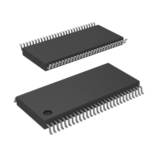
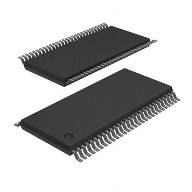
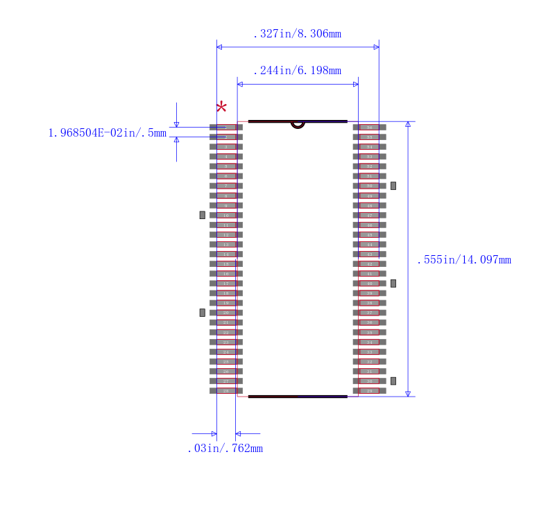
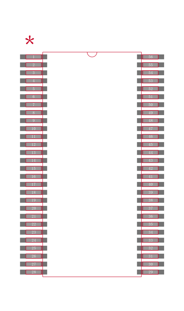
引脚数 56
封装 TSSOP-56
长度 14 mm
宽度 6.1 mm
高度 1.15 mm
封装 TSSOP-56
工作温度 -40℃ ~ 85℃ TA
产品生命周期 Active
包装方式 Tape & Reel TR
RoHS标准 RoHS Compliant
含铅标准 Lead Free
ECCN代码 EAR99
| 型号/品牌 | 代替类型 | 替代型号对比 |
|---|---|---|
SN74ALVCH16646DGGR TI 德州仪器 | 当前型号 | 当前型号 |
74ALVCH16646DGGRG4 德州仪器 | 完全替代 | SN74ALVCH16646DGGR和74ALVCH16646DGGRG4的区别 |
74ALVCH16646DGGRE4 德州仪器 | 完全替代 | SN74ALVCH16646DGGR和74ALVCH16646DGGRE4的区别 |