


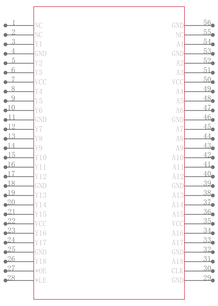
通用总线函数 18bit Univ Bus
A Dynamic Output Control DOC circuit is implemented, which, during the transition, initially lowers the output impedance to effectively drive the load and, subsequently, raises the impedance to reduce noise. Figure 1 shows typical VOL vs IOL and VOH vs IOH curves to illustrate the output impedance and drive capability of the circuit. At the beginning of the signal transition, the DOC circuit provides a maximum dynamic drive that is equivalent to a high-drive standard-output device. For more information, refer to the application reports, _AVC Logic Family Technology and Applications_, literature number SCEA006, and _Dynamic Output Control DOC Circuitry Technology and Applications_, literature number SCEA009.
This 18-bit universal bus driver is operational at 1.2-V to 3.6-V VCC, but is designed specifically for 1.65-V to 3.6-V VCC operation.
Data flow from A to Y is controlled by the output-enable OE\ input. The device operates in the transparent mode when the latch-enable LE\ input is low. The A data is latched if the clock CLK input is held at a high or low logic level. If LE\ is high, the A data is stored in the latch/flip-flop on the low-to-high transition of CLK. When OE\ is high, the outputs are in the high-impedance state.
To ensure the high-impedance state during power up or power down, OE\ should be tied to VCC through a pullup resistor; the minimum value of the resistor is determined by the current-sinking capability of the driver.
This device is fully specified for partial-power-down applications using Ioff. The Ioff circuitry disables the outputs, preventing damaging current backflow through the device when it is powered down.
电源电压DC 3.30 V, 3.60 V max
输出电流 12.0 mA
电路数 18 Bit
电压波节 3.30 V, 2.50 V, 1.80 V, 1.50 V, 1.20 V
工作温度Max 85 ℃
工作温度Min -40 ℃
电源电压 1.4V ~ 3.6V
安装方式 Surface Mount
引脚数 56
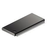
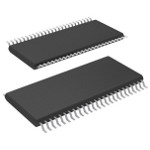
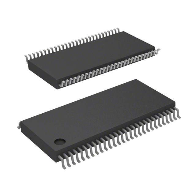
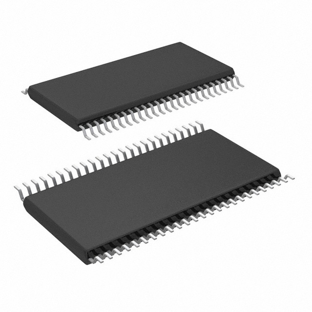
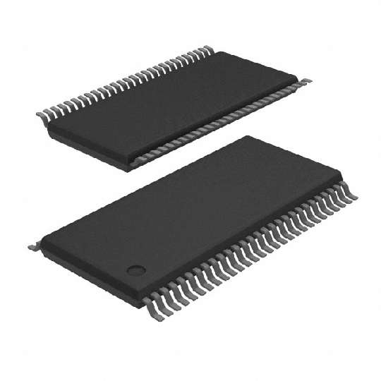
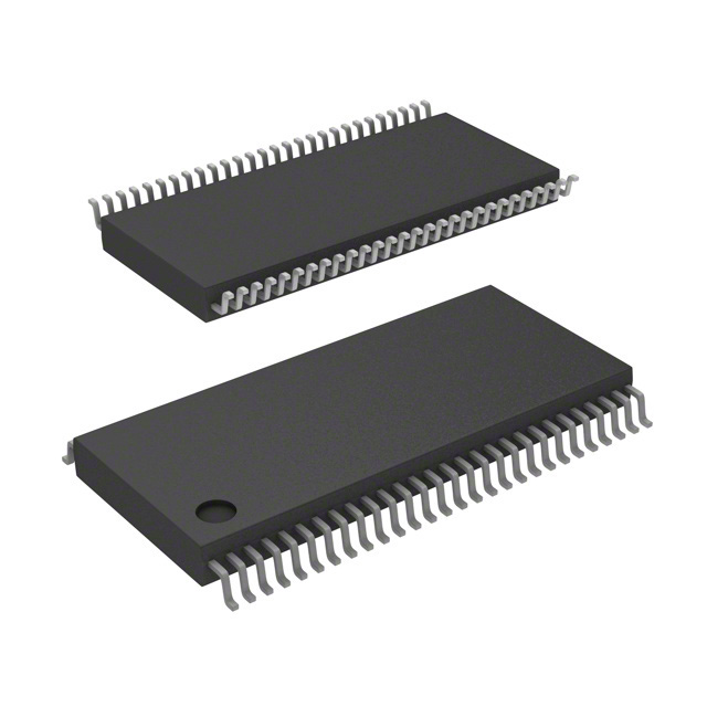
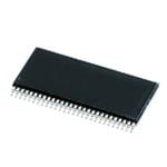
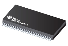
封装 TSSOP-56
长度 14 mm
宽度 6.1 mm
高度 1.05 mm
封装 TSSOP-56
工作温度 -40℃ ~ 85℃
产品生命周期 Active
包装方式 Tape & Reel TR
RoHS标准 RoHS Compliant
含铅标准 Lead Free
| 型号/品牌 | 代替类型 | 替代型号对比 |
|---|---|---|
SN74AVC16834DGGR TI 德州仪器 | 当前型号 | 当前型号 |
SN74AVC16834DGVR 德州仪器 | 完全替代 | SN74AVC16834DGGR和SN74AVC16834DGVR的区别 |
74AVC16834DGGRE4 德州仪器 | 类似代替 | SN74AVC16834DGGR和74AVC16834DGGRE4的区别 |
PI74AVC16834AE 百利通 | 功能相似 | SN74AVC16834DGGR和PI74AVC16834AE的区别 |