


通用总线函数 2.5/3.3V 18bit Univ
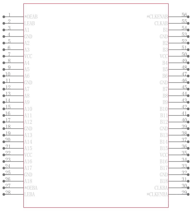
The "ALVTH16601 devices are 18-bit universal bus transceivers designed for 2.5-V or 3.3-V VCC operation, but with the capability to provide a TTL interface to a 5-V system environment.
The devices combine D-type latches and D-type flip-flops to allow data flow in transparent, latched, and clocked modes.
Data flow in each direction is controlled by output-enable OEAB\ and OEBA\\\\, latch-enable LEAB and LEBA, and clock CLKAB and CLKBA inputs. The clock can be controlled by the clock-enable CLKENAB\ and CLKENBA\\\\ inputs. For A-to-B data flow, the device operates in the transparent mode when LEAB is high. When LEAB is low, the A data is latched if CLKAB is held at a high or low logic level. If LEAB is low, the A data is stored in the latch/flip-flop on the low-to-high transition of CLKAB. Output enable OEAB\ is active low. When OEAB\ is low, the outputs are active. When OEAB\ is high, the outputs are in the high-impedance state.
Data flow for B to A is similar to that of A to B, but uses OEBA\, LEBA, CLKBA, and CLKENBA\\\\.
This device is fully specified for hot-insertion applications using Ioff and power-up 3-state. The Ioff circuitry disables the outputs, preventing damaging current backflow through the device when it is powered down. The power-up 3-state circuitry places the outputs in the high-impedance state during power up and power down, which prevents driver conflict.
When VCC is between 0 and 1.2 V, the device is in the high-impedance state during power up or power down. However, to ensure the high-impedance state above 1.2 V, OE\ should be tied to VCC through a pullup resistor; the minimum value of the resistor is determined by the current-sinking capability of the driver.
Active bus-hold circuitry is provided to hold unused or floating data inputs at a valid logic level.
The SN54ALVTH16601 is characterized for operation over the full military temperature range of -55°C to 125°C. The SN74ALVTH16601 is characterized for operation from -40°C to 85°C. View datasheet View product folder
电源电压DC 2.70 V, 3.60 V max
输出电流 32.0 mA
电路数 18 Bit
通道数 18
位数 18
电压波节 3.30 V, 2.50 V
工作温度Max 85 ℃
工作温度Min -40 ℃
电源电压 2.3V ~ 2.7V
安装方式 Surface Mount
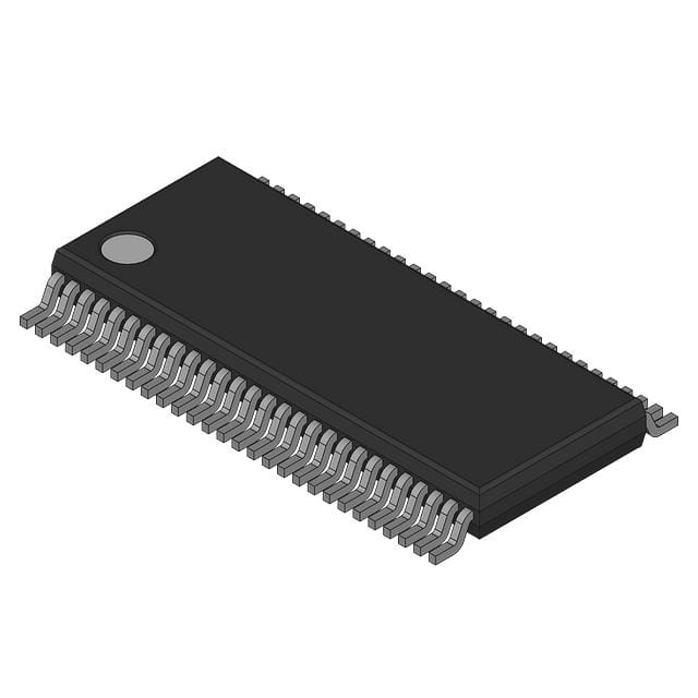
引脚数 56
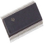
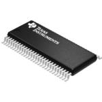
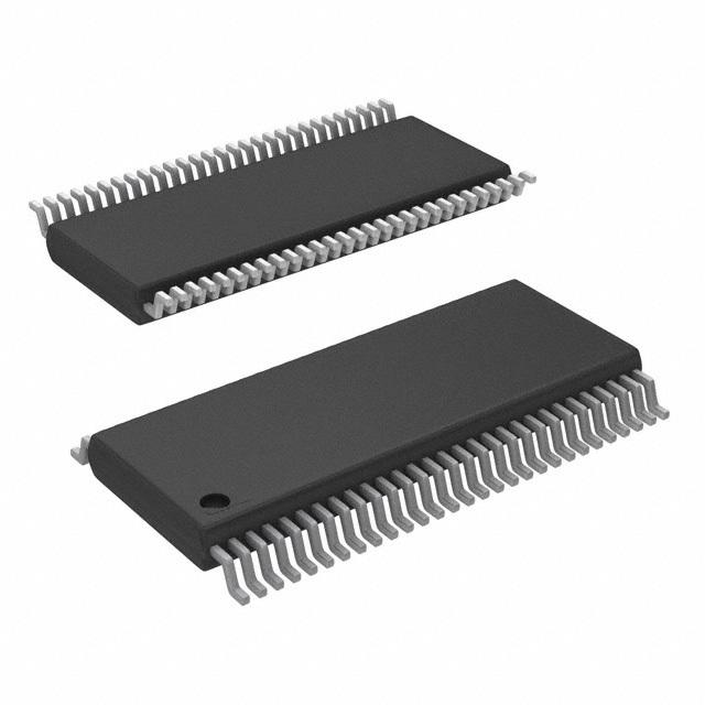
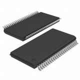
封装 TVSOP-56
长度 11.3 mm
宽度 4.4 mm
高度 1.05 mm
封装 TVSOP-56
工作温度 -40℃ ~ 85℃
产品生命周期 Active
包装方式 Tape & Reel TR
RoHS标准 RoHS Compliant
含铅标准 Lead Free
ECCN代码 EAR99
| 型号/品牌 | 代替类型 | 替代型号对比 |
|---|---|---|
SN74ALVTH16601VR TI 德州仪器 | 当前型号 | 当前型号 |
SN74ALVTH16601DLR 德州仪器 | 完全替代 | SN74ALVTH16601VR和SN74ALVTH16601DLR的区别 |
74ALVTH16601VRG4 德州仪器 | 类似代替 | SN74ALVTH16601VR和74ALVTH16601VRG4的区别 |