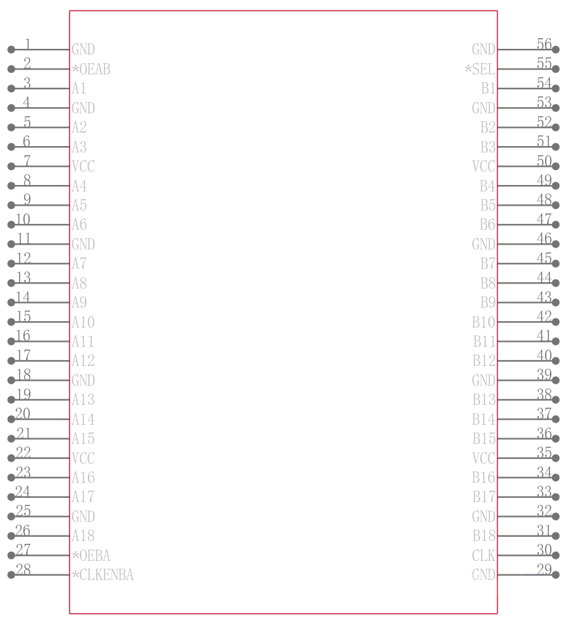

具有三态输出的18位寄存总线收发器 18-BIT REGISTERED BUS TRANSCEIVER WITH 3-STATE OUTPUTS
This 18-bit universal bus transceiver is designed for 1.65-V to 3.6-V VCC operation.
Data flow in each direction is controlled by output-enable OEAB\ and OEBA\\\\ and clock-enable CLKENBA\\\\ inputs. For the A-to-B data flow, the data flows through a single buffer. The B-to-A data can flow through a four-stage pipeline register path, or through a single register path, depending on the state of the select SEL\\\\ input.
Data is stored in the internal registers on the low-to-high transition of the clock CLK input, provided that the appropriate CLKENBA\ input is low. The B-to-A data transfer is synchronized with CLK.
To ensure the high-impedance state during power up or power down, OE\ should be tied to VCC through a pullup resistor; the minimum value of the resistor is determined by the current-sinking capability of the driver.
Active bus-hold circuitry holds unused or undriven inputs at a valid logic state. Use of pullup or pulldown resistors with the bus-hold circuitry is not recommended.
电源电压DC 1.65V ~ 3.60V
输出接口数 18
电路数 18 Bit
通道数 18
位数 18
电压波节 3.30 V, 2.70 V, 2.50 V, 1.80 V
工作温度Max 85 ℃
工作温度Min -40 ℃
电源电压 1.65V ~ 3.6V
电源电压Max 3.6 V
电源电压Min 1.65 V
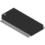
安装方式 Surface Mount
引脚数 56
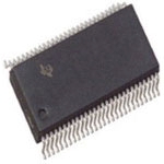
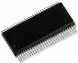
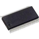
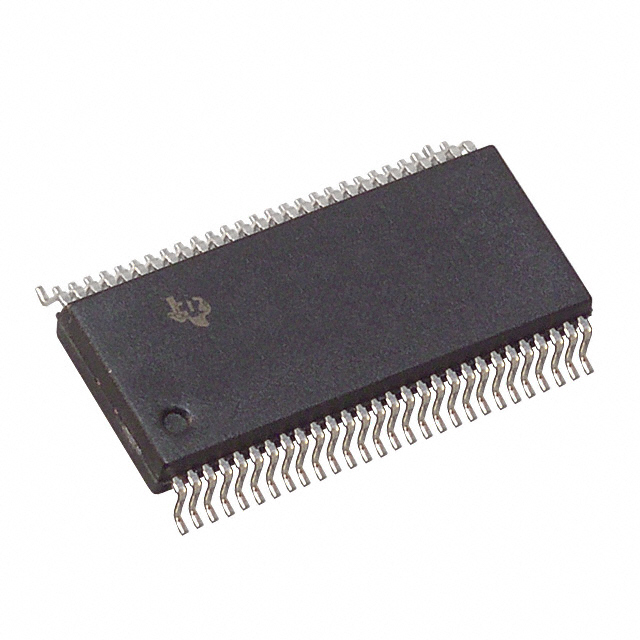
封装 SSOP-56
长度 18.41 mm
宽度 7.49 mm
高度 2.59 mm
封装 SSOP-56
工作温度 -40℃ ~ 85℃
产品生命周期 Active
包装方式 Tube
RoHS标准 RoHS Compliant
含铅标准 Lead Free
REACH SVHC标准 No SVHC
ECCN代码 EAR99