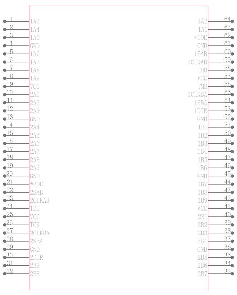

内置18位收发器和寄存器 WITH 18-BIT TRANSCEIVER AND REGISTER
This scan test device with a 18-bit bus transceiver and register is a member of the Texas Instruments SCOPE testability IC family. This device supports IEEE Std 1149.1-1990 boundary scan to facilitate testing of complex circuit board assemblies. Scan access to the test circuitry is accomplished via the four-wire test access port TAP interface.
In the normal mode, this device is an 18-bit bus transceiver and register that allows for multiplexed transmission of data directly from the input bus or from the internal registers. It can be used either as two 9-bit transceivers or one 18-bit transceiver. The test circuitry can be activated by the TAP to take snapshot samples of the data appearing at the device pins or to perform a self-test on the boundary test cells. Activating the TAP in the normal mode does not affect the functional operation of the SCOPE bus transceivers and registers.
Transceiver function is controlled by output-enable OE\ and direction DIR inputs. When OE\ is low, the transceiver is active and operates in the A-to-B direction when DIR is high or in the B-to-A direction when DIR is low. When OE\ is high, both the A and B outputs are in the high-impedance state, effectively isolating both buses.
Data flow is controlled by clock CLKAB and CLKBA and select SAB and SBA inputs. Data on the A bus is clocked into the associated registers on the low-to-high transition of CLKAB. When SAB is low, real-time A data is selected for presentation to the B bus transparent mode. When SAB is high, stored A data is selected for presentation to the B bus registered mode. The function of the CLKBA and SBA inputs mirrors that of CLKAB and SAB, respectively. Figure 1 illustrates the four fundamental bus-management functions that can be performed with the SN74ABT18646.
In the test mode, the normal operation of the SCOPE bus transceivers and registers is inhibited, and the test circuitry is enabled to observe and control the I/O boundary of the device. When enabled, the test circuitry can perform boundary scan test operations according to the protocol described in IEEE Std 1149.1-1990.
Four dedicated test pins are used to observe and control the operation of the test circuitry: test data input TDI, test data output TDO, test mode select TMS, and test clock TCK. Additionally, the test circuitry can perform other testing functions, such as parallel signature analysis on data inputs and pseudorandom pattern generation from data outputs. All testing and scan operations are synchronized to the TAP interface.
Additional flexibility is provided in the test mode through the use of two boundary scan cells BSCs for each I/O pin. This allows independent test data to be captured and forced at either bus A or B. A PSA/COUNT instruction is also included to ease the testing of memories and other circuits where a binary count addressing scheme is useful.