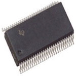
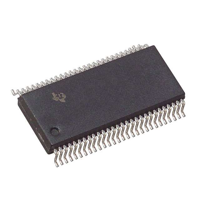
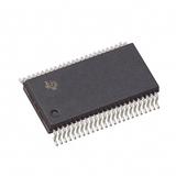

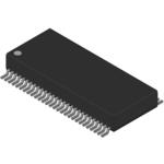
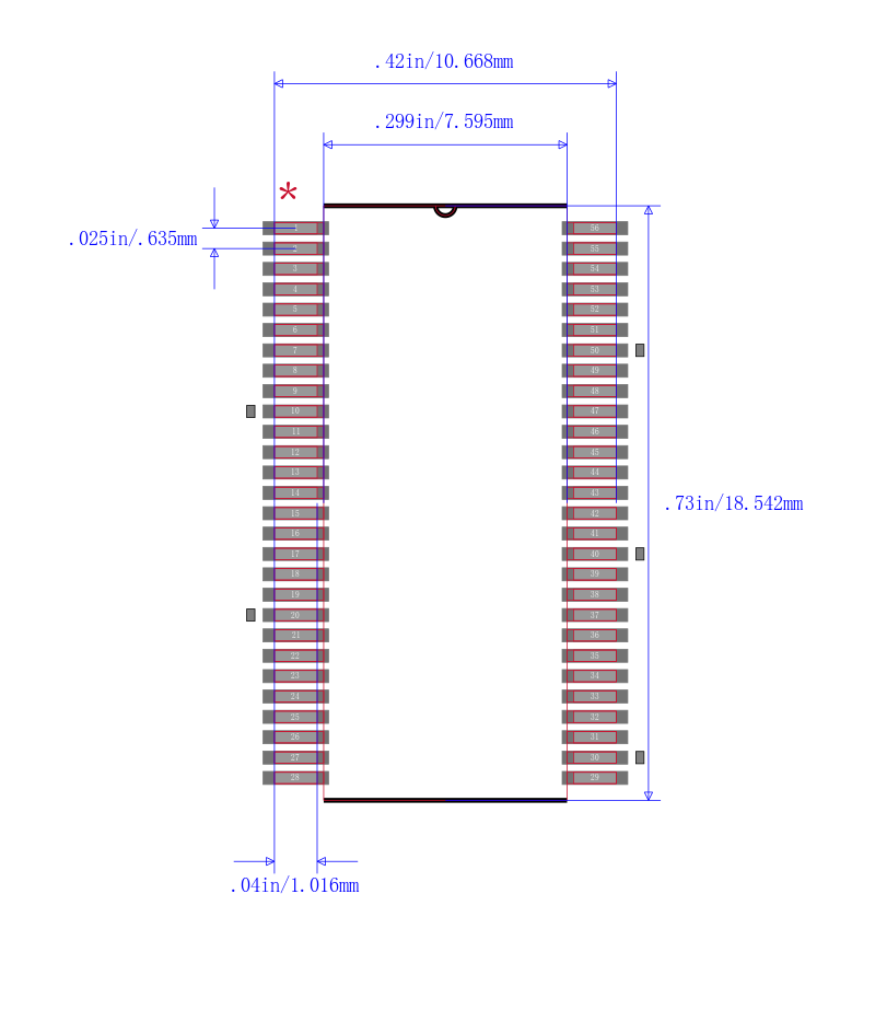
17位LVTTL - TO- GTL / GTL +通用总线,提供缓冲时钟输出收发器 17-BIT LVTTL-TO-GTL/GTL+ UNIVERSAL BUS TRANSCEIVER WITH BUFFERED CLOCK OUTPUTS
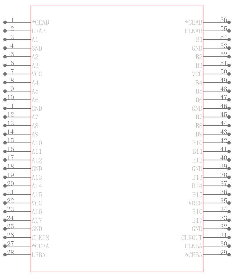
The SN74GTL16616 is a 17-bit UBT transceiver that provides LVTTL-to-GTL/GTL+ and GTL/GTL+-to-LVTTL signal-level translation. Combined D-type flip-flops and D-type latches allow for transparent, latched, clocked, and clocked-enabled modes of data transfer identical to the "16601 function. Additionally, this device provides for a copy of CLKAB at GTL/GTL+ signal levels CLKOUT and conversion of a GTL/GTL+ clock to LVTTL logic levels CLKIN. This device provides an interface between cards operating at LVTTL logic levels and a backplane operating at GTL/GTL+ signal levels. Higher-speed operation is a direct result of the reduced output swing <1 V, reduced input threshold levels, and OEC circuitry.
The user has the flexibility of using this device at either GTL VTT = 1.2 V and VREF = 0.8 V or the preferred higher noise margin GTL+ VTT = 1.5 V and VREF = 1 V signal levels. GTL+ is the Texas Instruments derivative of the Gunning Transceiver Logic GTL JEDEC standard JESD 8-3. The B port normally operates at GTL or GTL+ signal levels, while the A-port and control inputs are compatible with LVTTL logic levels and are 5-V tolerant. V REF is the reference input voltage for the B port. VCC 5 V supplies the internal and GTL circuitry while VCC 3.3 V supplies the LVTTL output buffers.
Data flow in each direction is controlled by output-enable OEAB\ and OEBA\\\\, latch-enable LEAB and LEBA, and clock CLKAB and CLKBA inputs. The clock can be controlled by the clock-enable CEAB\ and CEBA\\\\ inputs. For A-to-B data flow, the device operates in the transparent mode when LEAB is high. When LEAB is low, the A data is latched if CEAB\ is low and CLKAB is held at a high or low logic level. If LEAB is low, the A-bus data is stored in the latch/flip-flop on the low-to-high transition of CLKAB if CEAB\ also is low. When OEAB\ is low, the outputs are active. When OEAB\ is high, the outputs are in the high-impedance state. Data flow for B to A is similar to that of A to B, but uses OEBA\, LEBA, CLKBA, and CEBA\\\\.
This device is fully specified for partial-power-down applications using Ioff. The Ioff circuitry disables the outputs, preventing damaging current backflow through the device when it is powered down.
Active bus-hold circuitry holds unused or undriven LVTTL inputs at a valid logic state. Use of pullup or pulldown resistors with the bus-hold circuitry is not recommended.
To ensure the high-impedance state during power up or power down, OE\ should be tied to VCC through a pullup resistor; the minimum value of the resistor is determined by the current-sinking capability of the driver. View datasheet View product folder
| 型号/品牌 | 代替类型 | 替代型号对比 |
|---|---|---|
SN74GTL16616DLR TI 德州仪器 | 当前型号 | 当前型号 |
SN74GTL16616DL 德州仪器 | 完全替代 | SN74GTL16616DLR和SN74GTL16616DL的区别 |
SN74GTL16616DLG4 德州仪器 | 类似代替 | SN74GTL16616DLR和SN74GTL16616DLG4的区别 |