

与PRECHAGED产出2.5V / 3.3V低电压高带宽总线开关10位FET总线开关 10 BIT FET BUS SWITCH WITH PRECHAGED OUTPUTS 2.5V/3.3V LOW VOLTAGE HIGH BANDWIDTH BUS SWITCH
The SN74CB3Q6800 is a high-bandwidth FET bus switch utilizing a charge pump to elevate the gate voltage of the pass transistor, providing a low and flat ON-state resistance ron. The low and flat ON-state resistance allows for minimal propagation delay and supports rail-to-rail switching on the data input/output I/O ports. The device also features low data I/O capacitance to minimize capacitive loading and signal distortion on the data bus. Specifically designed to support high-bandwidth applications, the SN74CB3Q6800 provides an optimized interface solution ideally suited for broadband communications, networking, and data-intensive computing systems.
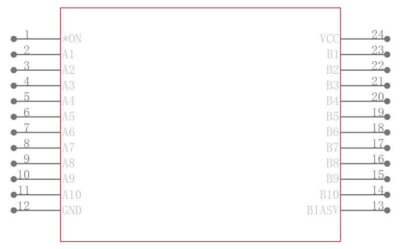
The SN74CB3Q6800 is a 10-bit bus switch with a single output-enable ON\\\\ input. When ON\ is low, the 10-bit bus switch is ON and the A port is connected to the B port, allowing bidirectional data flow between ports. When ON\ is high, the 10-bit bus switch is OFF and a high-impedance state exists between the A and B ports. The B port is precharged to bias voltage BIASV through the equivalent of a 10-k resistor when ON\ is high, or if the device is powered down VCC = 0 V.
During insertion or removal of a card into or from an active bus, the cards output voltage may be close to GND. When the connector pins make contact, the cards parasitic capacitance tries to force the bus signal to GND, creating a possible glitch on the active bus. This glitching effect can be reduced by using a bus switch with precharged bias voltage BIASV of the bus switch equal to the input threshold voltage level of the receivers on the active bus. This method will ensure that any glitch produced by insertion or removal of the card will not cross the input threshold region of the receivers on the active bus, minimizing the effects of live-insertion noise.
This device is fully specified for partial-power-down applications using Ioff. The Ioff circuitry prevents damaging current backflow through the device when it is powered down. The device has isolation during power off.
To ensure the high-impedance state during power up or power down, ON\ should be tied to VCC through a pullup resistor; the minimum value of the resistor is determined by the current-sinking capability of the driver.
电源电压DC 2.30V ~ 3.60V
输出电流 30.0 mA
触点类型 SPST
位数 10
传送延迟时间 225 ps
电压波节 2.50 V, 3.30 V
静态电流 750 µA
带宽 500 MHz
工作温度Max 85 ℃
工作温度Min -40 ℃
电源电压 2.3V ~ 3.6V
安装方式 Surface Mount
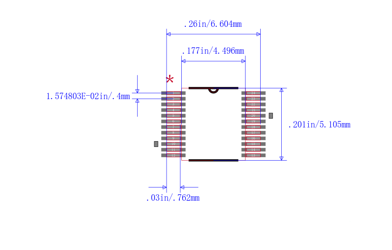
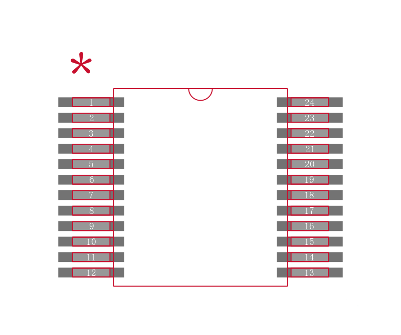
引脚数 24
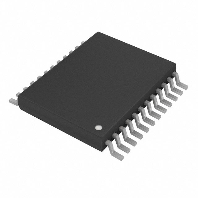
封装 TVSOP-24
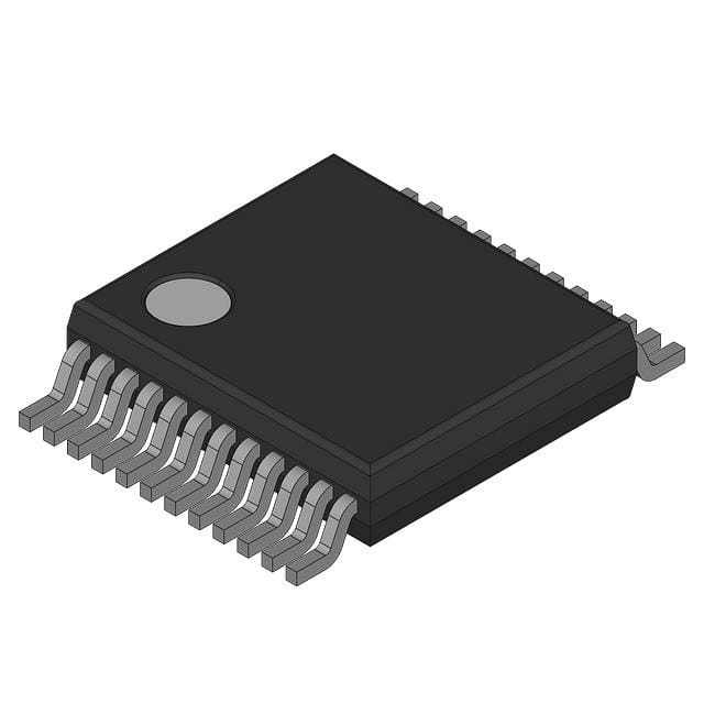
封装 TVSOP-24
工作温度 -40℃ ~ 85℃
产品生命周期 Active
包装方式 Tape & Reel TR
RoHS标准 RoHS Compliant
含铅标准 Lead Free
| 型号/品牌 | 代替类型 | 替代型号对比 |
|---|---|---|
SN74CB3Q6800DGVR TI 德州仪器 | 当前型号 | 当前型号 |
SN74CB3Q6800PWR 德州仪器 | 完全替代 | SN74CB3Q6800DGVR和SN74CB3Q6800PWR的区别 |
SN74CB3Q6800PWG4 德州仪器 | 完全替代 | SN74CB3Q6800DGVR和SN74CB3Q6800PWG4的区别 |
74CB3Q6800DGVRG4 德州仪器 | 完全替代 | SN74CB3Q6800DGVR和74CB3Q6800DGVRG4的区别 |