1 - OF- 8场效应管复用器/解复用器2.5 V / 3.3 V低电压,高带宽总线开关 1-OF-8 FET MULTIPLEXER/DEMULTIPLEXER 2.5-V/3.3-V LOW-VOLTAGE, HIGH-BANDWIDTH BUS SWITCH
The SN74CB3Q3251 is a high-bandwidth FET bus switch utilizing a charge pump to elevate the gate voltage of the pass transistor, providing a low and flat ON-state resistance ron. The low and flat ON-state resistance allows for minimal propagation delay and supports rail-to-rail switching on the data input/output I/O ports. The device also features low data I/O capacitance to minimize capacitive loading and signal distortion on the data bus. Specifically designed to support high-bandwidth applications, the SN74CB3Q3251 provides an optimized interface solution ideally suited for broadband communications, networking, and data-intensive computing systems.
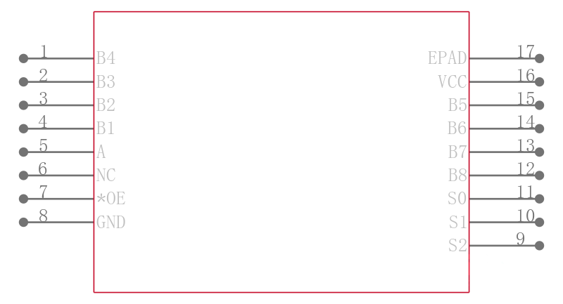
The SN74CB3Q3251 is a 1-of-8 multiplexer/demultiplexer with a single output-enable OE\\\\ input. The select S0, S1, S2 inputs control the data path of the multiplexer/demultiplexer. When OE\ is low, the multiplexer/demultiplexer is enabled, and the A port is connected to the B port, allowing bidirectional data flow between ports. When OE\ is high, the multiplexer/demultiplexer is disabled, and a high-impedance state exists between the A and B ports.
This device is fully specified for partial-power-down applications using Ioff. The Ioff circuitry prevents damaging current backflow through the device when it is powered down. The device has isolation during power off.
To ensure the high-impedance state during power up or power down, OE\ should be tied to VCC through a pullup resistor; the minimum value of the resistor is determined by the current-sinking capability of the driver.
输出接口数 1
通道数 8
位数 8
传送延迟时间 120 ps
电压波节 2.50 V, 3.30 V
带宽 500 MHz
输入数 8
工作温度Max 85 ℃
工作温度Min -40 ℃
电源电压 2.3V ~ 3.6V
电源电压Max 3.6 V
电源电压Min 2.3 V
安装方式 Surface Mount
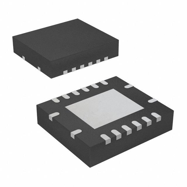
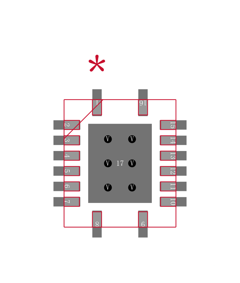
引脚数 16
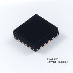
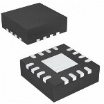
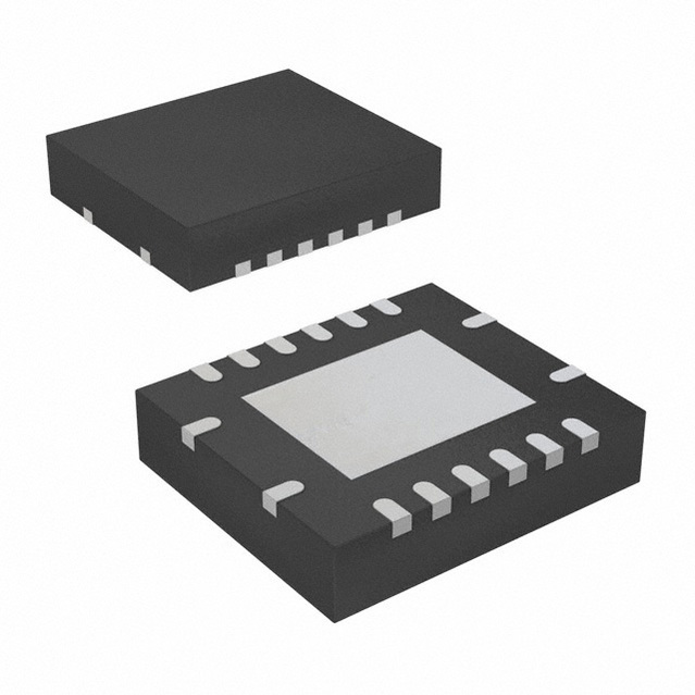
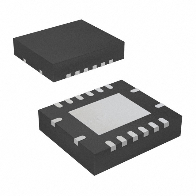
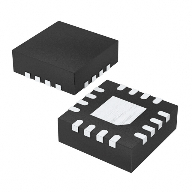
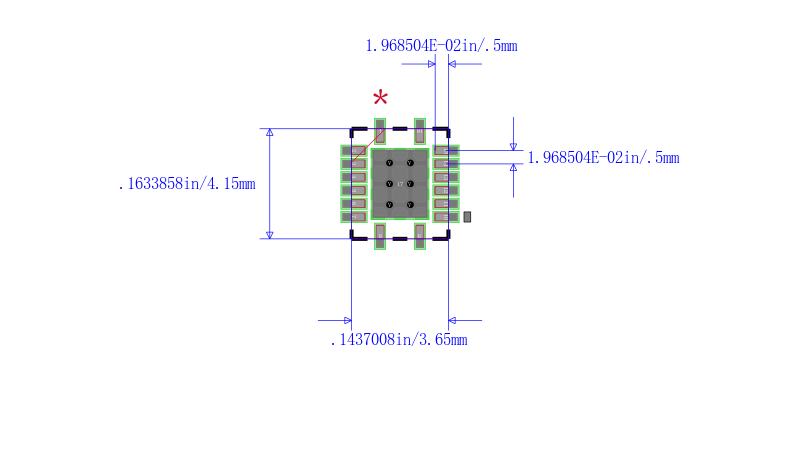
封装 VQFN-16
长度 4 mm
宽度 3.5 mm
高度 0.8 mm
封装 VQFN-16
工作温度 -40℃ ~ 85℃
产品生命周期 Active
包装方式 Tape & Reel TR
RoHS标准 RoHS Compliant
含铅标准 Lead Free
ECCN代码 EAR99
| 型号/品牌 | 代替类型 | 替代型号对比 |
|---|---|---|
SN74CB3Q3251RGYR TI 德州仪器 | 当前型号 | 当前型号 |
SN74CB3Q3251PW 德州仪器 | 完全替代 | SN74CB3Q3251RGYR和SN74CB3Q3251PW的区别 |
SN74CB3Q3257RGYR 德州仪器 | 类似代替 | SN74CB3Q3251RGYR和SN74CB3Q3257RGYR的区别 |